ECE 5745 Section 2: ASIC Flow Back-End
- Author: Christopher Batten
- Date: February 4, 2022
Table of Contents
- Introduction
- NanGate 45nm Standard-Cell Libraries
- Revisiting the ASIC Flow Front-End
- Using Cadence Innovus for Place-and-Route
- Using Synopsys VCS for Back-Annotated Gate-Level Simulation
Introduction
In this section, we will be discussing the back-end of the ASIC toolflow. More detailed tutorials will be posted on the public course website shortly, but this section will at least give you a chance to take a gate-level netlist through place-and-route and energy analysis. The following diagram illustrates the tool flow we will be using in ECE 5745 along. Notice that the Synopsys and Cadence ASIC tools all require various views from the standard-cell library which part of the ASIC design kit (ADK).
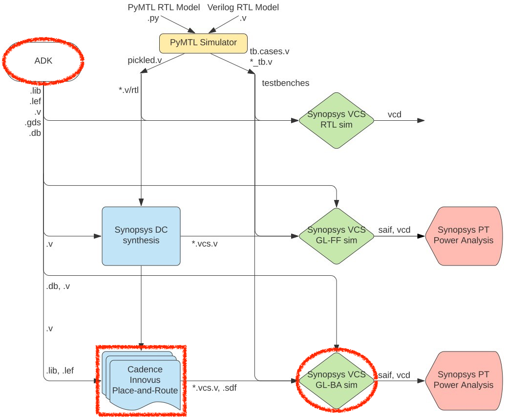
The “back-end” of the flow is highlighted in red and refers to Cadence Innovus and Synopsys VCS.
-
We use Cadence Innovus to place-and-route our design, which means to place all of the gates in the gate-level netlist into rows on the chip and then to generate the metal wires that connect all of the gates together. We need to provide Cadence Innovus with similar abstract logical and timing views used in Synopsys DC. Cadence Innovus takes as input the
.libfile which is the ASCII text version of a.dbfile. In addition, we need to provide Cadence Innovus with technology information in.lefand.captableformat and abstract physical views of the standard-cell library in.lefformat. Cadence Innovus will generate an updated Verilog gate-level netlist, a.speffile which contains parasitic resistance/capacitance information about all nets in the design, and a.gdsfile which contains the final layout. The.gdsfile can be inspected using the open-source Klayout GDS viewer. Cadence Innovus also generates reports which can be used to accurately characterize area and timing. -
We use Synopsys VCS for back-annotated gate-level simulation. Gate-level simulation involves simulating every standard-cell gate and helps verify that the Verilog gate-level netlist is functionally correct. Fast-functional gate-level simulation does not include any timing information, while back-annotated gate-levle simulation does include the estimated delay of every gate and every wire.
Extensive documentation is provided by Synopsys and Cadence. We have organized this documentation and made it available to you on the Canavas course page:
The first step is to access ecelinux. You can use VS Code for
working at the command line, but you will also need to a remote access
option that supports Linux applications with a GUI such as X2Go,
MobaXterm, or Mac Terminal with XQuartz. Once you are at the ecelinux
prompt, source the setup script, clone this repository from GitHub, and
define an environment variable to keep track of the top directory for the
project.
% source setup-ece5745.sh
% mkdir -p $HOME/ece5745
% cd $HOME/ece5745
% git clone git@github.com:cornell-ece5745/ece5745-S02-back-end sec2
% cd sec2
% TOPDIR=$PWD
NanGate 45nm Standard-Cell Libraries
Recall that a standard-cell library is a collection of combinational and
sequential logic gates that adhere to a standardized set of logical,
electrical, and physical policies. For example, all standard cells are
usually the same height, include pins that align to a predetermined
vertical and horizontal grid, include power/ground rails and nwells in
predetermined locations, and support a predetermined number of drive
strengths. In this course, we will be using the a NanGate 45nm
standard-cell library. It is based on a “fake” 45nm technology. This
means you cannot actually tapeout a design using this standard cell
library, but the technology is representative enough to provide
reasonable area, energy, and timing estimates for teaching purposes. All
of the files associated with this standard cell library are located in
the $ECE5745_STDCELLS directory.
Let’s look at some layout for the standard cell library just like we did in the last section.
% klayout -l $ECE5745_STDCELLS/klayout.lyp $ECE5745_STDCELLS/stdcells.gds
Let’s look at a 3-input NAND cell, find the NAND3X1 cell in the left-hand cell list, and then choose _Display > Show as New Top from the menu. We will learn more about layout and how this layout corresponds to a static CMOS circuit later in the course. The key point is that the layout for the standard cells are the basic building blocks that we will be using to create our ASIC chips.
The Synopsys and Cadence tools do not actually use this layout directly;
it is actually too detailed. Instead these tools use abstract views of
the standard cells, which capture logical functionality, timing,
geometry, and power usage at a much higher level. In the last section, we
looked at Verilog and .lib views. The back-end flow takes as input the
.lib view for logical timing information, but it also takes as input a
.lef view which contains physical information about the standard
cell. Let’s look at the LEF for the 3-input NAND cell.
% less -p NAND3_X1 $ECE5745_STDCELLS/stdcells.lef
The .lef view includes information about the size of the standard cell,
but also includes information about where every pin is physically
located. You can use Klayout to view .lef files as well. Start Klayout
like this:
% klayout
Choose File > Import > LEF from the menu. Navigate to the cells.lef
file which is located here:
/classes/ece5745/install/adk-pkgs/freepdk-45nm/stdview/stdcells.lef
Let’s look at a 3-input NAND cell, find the NAND3X1 cell in the
left-hand cell list, and then choose _Display > Show as New Top from the
menu. The .lef file does not contain any transistor-level information.
It only contains information relevant to placement and routing.
In addition to physical information about each standard cell, the back-end flow also needs to take as input general information about the technology. This information is contained in two files:
% less $ECE5745_STDCELLS/rtk-tech.lef
% less $ECE5745_STDCELLS/rtk-typical.captable
The first provides information about the geometry and orientation of wires for each metal layer. The second provides information about the resistance and capacitance of each metal layer.
Now that we have looked at the physical views of the standard cell library, we can now try using these views and the ASIC flow back-end to place and route a gate-level netlist.
Revisiting the ASIC Flow Front-End
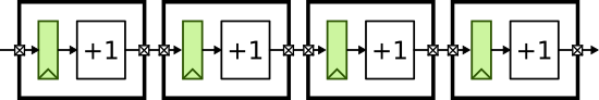
As in the last section, we will be using the following four-stage registered incrementer as our example design:
Before we can place and route a gate-level netlist, we need to synthesize that netlist. This is what we learned about in the last section. Here are the steps to test and then synthesize the design using Synopsys DC.
Test, Simulate, and Translate the Four-Stage Registered Incrementer
Always run the tests before pushing anything through the ASIC flow. There is no sense in running the flow if the design is incorrect!
% mkdir -p $TOPDIR/sim/build
% cd $TOPDIR/sim/build
% pytest ../tut3_verilog/regincr
Next we should rerun all the tests with the --test-verilog and
--dump-vtb command line options to ensure that the design also works
after translated into Verilog and that we generate a Verilog test-bench
for gate-level simulation. You should do this step even if you are using
Verilog for your RTL design.
% cd $TOPDIR/sim/build
% pytest ../tut3_verilog/regincr --test-verilog --dump-vtb
The tests are for verification. When we push a design through the flow we want to use a simulator which is focused on evaluation. You can run the simulator for our four-stage registered incrementer like this:
% cd $TOPDIR/sim/build
% ../tut3_verilog/regincr/regincr-sim 0x10 0x20 0x30 0x40
% less RegIncrNstage__p_nstages_4__pickled.v
You should now have the Verilog that we want to push through the ASIC flow.
Synthesize Verilog RTL to a Verilog Gate-Level Netlist
We start by creating a subdirectory for our work, and then launching Synopsys DC.
% mkdir -p $TOPDIR/asic/synopsys-dc-synth
% cd $TOPDIR/asic/synopsys-dc-synth
% dc_shell-xg-t
We used the following commands in the last discussion section:
dc_shell> set_app_var target_library "$env(ECE5745_STDCELLS)/stdcells.db"
dc_shell> set_app_var link_library   "* $env(ECE5745_STDCELLS)/stdcells.db"
dc_shell> analyze -format sverilog ../../sim/build/RegIncrNstage__p_nstages_4__pickled.v
dc_shell> elaborate RegIncrNstage__p_nstages_4
dc_shell> check_design
dc_shell> create_clock clk -name ideal_clock1 -period 1
dc_shell> compile
dc_shell> write -format verilog -hierarchy -output post-synth.v
dc_shell> write -format ddc     -hierarchy -output post-synth.ddc
dc_shell> exit
To simplify this process, we have provided you a TCL file that includes these commands. You can run this TCL script using Synopsys DC like this:
% cd $TOPDIR/asic/synopsys-dc-synth
% dc_shell-xg-t -f run.tcl
Take a few minutes to examine the resulting Verilog gate-level netlist. Notice that the module hierarchy is preserved.
% less post-synth.v
This is the gate-level netlist that we now want to place and route.
Using Cadence Innovus for Place-and-Route
We will be running Cadence Innovus in a separate directory to keep the input and output files separate.
% mkdir -p $TOPDIR/asic/cadence-innovus-pnr
% cd $TOPDIR/asic/cadence-innovus-pnr
Before starting Cadence Innovus, we need to create two files which will
be loaded into the tool. The first file is a .sdc file which contains
timing constraint information about our design. This file is where we
specify our target clock period, but it is also where we could specify
input or output delay constraints (e.g., the output signals must be
stable 200ps before the rising edge). Use your favorite text editor to
create a file named constraints.sdc in
$TOPDIR/asic/cadence-innovus-pnr with the following content:
create_clock clk -name ideal_clock -period 1
The create_clock command is similar to the command we used in
synthesis, and usually, we use the same target clock period that we used
for synthesis. In this case, we are targeting a 1GHz clock frequency
(i.e., a 1ns clock period).
The second file is a “multi-mode multi-corner” (MMMC) analysis file. This
file specifies what “corner” to use for our timing analysis. A corner is
a characterization of the standard cell library and technology with
specific assumptions about the process temperature, and voltage (PVT). So
we might have a “fast” corner which assumes best-case process
variability, low temperature, and high voltage, or we might have a “slow”
corner which assumes worst-case variability, high temperature, and low
voltage. To ensure our design worked across a range of operating
conditions, we need to evaluate our design across a range of corners. In
this course, we will keep things simple by only considering a “typical”
corner (i.e., average PVT). Use Geany or your favorite text editor to
create a file named setup-timing.tcl in
$TOPDIR/asic/cadence-innovus-pnr with the following content:
create_rc_corner -name typical \
   -cap_table "$env(ECE5745_STDCELLS)/rtk-typical.captable" \
   -T 25

create_library_set -name libs_typical \
   -timing [list "$env(ECE5745_STDCELLS)/stdcells.lib"]

create_delay_corner -name delay_default \
   -early_library_set libs_typical \
   -late_library_set libs_typical \
   -rc_corner typical

create_constraint_mode -name constraints_default \
   -sdc_files [list constraints.sdc]

create_analysis_view -name analysis_default \
   -constraint_mode constraints_default \
   -delay_corner delay_default

set_analysis_view \
   -setup [list analysis_default] \
   -hold [list analysis_default]
The create_rc_corner command loads in the .captable file that we
examined earlier. This file includes information about the resistance and
capacitance of every metal layer. Notice that we are loading in the
“typical” captable and we are specifying an “average” operating
temperature of 25 degC. The create_library_set command loads in the
.lib file that we examined in the last section. This file includes
information about the input/output capacitance of each pin in each
standard cell along with the delay from every input to every output in
the standard cell. The create_delay_corner specifies a specific corner
that we would like to use for our timing analysis by putting together a
.captable and a .lib file. In this specific example, we are creating
a typical corner by putting together the typical .captable and typical
.lib we just loaded. The create_constraint_mode command loads in the
.sdc file we mentioned earlier in this section. The
create_analysis_view command puts together constraints with a specific
corner, and the set_analysis_view command tells Cadence Innovus that we
would like to use this specific analysis view for both setup and hold
time analysis.
Now that we have created our constraints.sdc and setup-timing.tcl
files we can start Cadence Innovus:
% innovus -64
This will launch the GUI. We can enter commands in the terminal and watch
the effect of these commands on our design in the GUI. We need to set
various variables before starting to work in Cadence Innovus. These
variables tell Cadence Innovus the location of the MMMC file, the
location of the Verilog gate-level netlist, the name of the top-level
module in our design, the location of the .lef files, and finally the
names of the power and ground nets.
innovus> set init_mmmc_file "setup-timing.tcl"
innovus> set init_verilog   "../synopsys-dc-synth/post-synth.v"
innovus> set init_top_cell  "RegIncrNstage__p_nstages_4"
innovus> set init_lef_file  "$env(ECE5745_STDCELLS)/rtk-tech.lef $env(ECE5745_STDCELLS)/stdcells.lef"
innovus> set init_gnd_net   "VSS"
innovus> set init_pwr_net   "VDD"
We can now use the init_design command to read in the verilog, set the
design name, setup the timing analysis views, read the technology .lef
for layer information, and read the standard cell .lef for physical
information about each cell used in the design.
innovus> init_design
We start by working on power planning which is the process of routing the
power and ground signals across the chip. First, we use the floorPlan
command to set the dimensions for our chip.
innovus> floorPlan -su 1.0 0.70 4.0 4.0 4.0 4.0
In this example, we have chosen the aspect ration to be 1.0, the target cell utilization to be 0.7, and we have added 4.0um of margin around the top, bottom, left, and right of the chip. This margin gives us room for the power ring which will go around the entire chip.
Often when working with the ASIC flow back-end, we need to explicitly
tell the tools how the logical design connects to the physical aspects of
the chip. For example, the next step is to tell Cadence Innovus that
VDD and VSS in the gate-level netlist correspond to the physical pins
labeled VDD and VSS in the .lef files.
innovus> globalNetConnect VDD -type pgpin -pin VDD -inst * -verbose
innovus> globalNetConnect VSS -type pgpin -pin VSS -inst * -verbose
The next step in power planning is to draw M1 wires for the power and ground rails that go along each row of standard cells.
innovus> sroute -nets {VDD VSS}
Now we create a power ring around our chip using the addRing command. A
power ring ensures we can easily get power and ground to all standard
cells. The command takes parameters specifying the width of each wire in
the ring, the spacing between the two rings, and what metal layers to use
for the ring.
innovus> addRing -nets {VDD VSS} -width 0.6 -spacing 0.5 \
                 -layer [list top 7 bottom 7 left 6 right 6]
We have power and ground rails along each row of standard cells and a
power ring, so now we need to hook these up. We can use the addStripe
command to draw wires and automatically insert vias whenever wires cross.
First we draw the vertical “stripes”.
innovus> addStripe -nets {VSS VDD} -layer 6 -direction vertical \
                   -width 0.4 -spacing 0.5 -set_to_set_distance 5 -start 0.5
And then we draw the horizontal “stripes”.
innovus> setAddStripeMode -stacked_via_bottom_layer 6 \
                   -stacked_via_top_layer    7

innovus> addStripe -nets {VSS VDD} -layer 7 -direction horizontal \
                   -width 0.4 -spacing 0.5 -set_to_set_distance 5 -start 0.5
Now that we have finished our basic power planning we can do the initial
placement and routing of the standard cells using the place_design
command:
innovus> place_design
You should be able to see the standard cells placed in the rows along with preliminary routing to connect all of the standard cells together. You can toggle the visibility of metal layers by pressing the number keys on the keyboard. So try toggling the visibility of M1, M2, M3, etc. You can visualize how the modules in the original Verilog mapped to the place-and-routed design by using the Design Browser. Choose the Windows > Workspaces > Design Browser + Physical menu option. Then use the Design Browser to click on specific modules or nets to highlight them in the physical view.
The place_design command will perform a very preliminary route to help
ensure a good placement, but we will now do a more detailed routing pass
for the clock and signals to improve the quality of results. The
cccopt_design command will do clock tree synthesis optimization to
improve the quality of the clock tree (e.g., less clock skew across the
chip). Before running the command make sure you can see the physical view
of the chip, and then watch how the clock net changes after the command
is complete. You can choose to just show the clock by changing the
visibility of nets in the right-hand panel.
innovus> ccopt_design
We can use the routeDesign to do detailed timing-driven routing of all
of the signals. As before, make sure you watch the physical view to see
the result before and after running this command. You should be able to
appreciate that the final result requires fewer and shorter wires.
innovus> routeDesign
The final step is to insert “filler” cells. Filler cells are essentially empty standard cells whose sole purpose is to connect the wells across each standard cell row.
innovus> setFillerMode -corePrefix FILL -core "FILLCELL_X4 FILLCELL_X2 FILLCELL_X1"
innovus> addFiller
Now we are basically done! Obviously there are many more steps required before you can really tape out a chip. We would need to add an I/O ring to connect the chip to the package, we would need to do further verification, and additional optimization.
For example, one thing we want to do is verify that the gate-level
netlist matches what is really in the final layout. We can do this using
the verifyConnectivity command. We can also do a preliminary “design
rule check” to make sure that the generated metal interconnect does not
violate any design rules with the verify_drc command.
innovus> verifyConnectivity
innovus> verify_drc
Now we can generate various artifacts. We might want to save the final gate-level netlist for the chip since Cadence Innovus will often insert new cells or change cells during its optimization passes.
innovus> saveNetlist post-pnr.v
We can also extract resistance and capacitance for the metal interconnect
and write this to a special .spef file and .sdf file. These files can
be used for later timing and/or power analysis.
innovus> extractRC
innovus> rcOut -rc_corner typical -spef typical.spef
innovus> write_sdf post-pnr.sdf -interconn all -setuphold split
And of course the step is to generate the real layout as a .gds file.
This is what we will send to the foundry when we are ready to tapeout the
chip.
innovus> streamOut post-pnr.gds \
           -merge "$env(ECE5745_STDCELLS)/stdcells.gds" \
           -mapFile "$env(ECE5745_STDCELLS)/rtk-stream-out.map"
We can also use Cadence Innovus to do timing, area, and power analysis similar to what we did with Synopsys DC. These post-place-and-route results will be much more accurate than the preliminary post-synthesis results.
innovus> report_timing
innovus> report_area
innovus> report_power -hierarchy all
Finally, we go ahead and exit Cadence Innovus.
innovus> exit
If you want you can open up the final layout using Klayout.
% klayout -l $ECE5745_STDCELLS/klayout.lyp post-pnr.gds
Choose Display > Full Hierarchy from the menu to display the entire design. Zoom in and out to see the individual transistors as well as the entire chip.
Using Synopsys VCS for Back-Annotated Gate-Level Simulation
As we learned in the last discussion section, good ASIC designers are always paranoid and never trust their tools. How do we know that the final post-place-and-route gate-level netlist is correct? Once again, we can rerun our test suite on the gate-level model. We can do this using Synopsys VCS for back-annotated gatel-level simulation. Back-annotated refers to the fact that this simulation will take into account all of the gate and interconnect delays. So this also helps build our confidence not just that the final gate-level netlist is functionally correct, but also that it meets all setup and hold time constraints. Here is how to run VCS for RTL simulation:
% mkdir -p $TOPDIR/asic/synopsys-vcs-bagl-sim
% cd $TOPDIR/asic/synopsys-vcs-bagl-sim
% vcs -full64 -sverilog +lint=all -xprop=tmerge -override_timescale=1ns/1ps \
    +incdir+../../sim/build \
    +vcs+dumpvars+vcs-bagl-sim.vcd \
    -top RegIncrNstage__p_nstages_4_tb \
    +define+CYCLE_TIME=1.0 \
    +define+VTB_INPUT_DELAY=0.1 \
    +define+VTB_OUTPUT_ASSERT_DELAY=0.99 \
    +neg_tchk +sdfverbose \
    -sdf max:RegIncrNstage__p_nstages_4_tb.DUT:../cadence-innovus-pnr/post-pnr.sdf \
    ../cadence-innovus-pnr/post-pnr.v \
    $ECE5745_STDCELLS/stdcells.v \
    ../../sim/build/RegIncrNstage__p_nstages_4_test_random_4_tb.v
This is a pretty long command line! So we provide you a shell script that has the command ready for you to use.
% cd $TOPDIR/asic/synopsys-vcs-bagl-sim
% source run-1ns.sh
You should see a simv binary which is the compiled RTL simulator which
you can run like this:
% cd $TOPDIR/asic/synopsys-vcs-bagl-sim
% ./simv
It should pass the test. Now let’s look at the resulting waveforms.
% cd $TOPDIR/asic/synopsys-vcs-bagl-sim
% gtkwave vcs-bagl-sim.vcd
Browse the signal hierarchy and display all the waveforms for the DUT using these steps:
- Expand out the signal tree until you find the DUT module
- Select the clk, in, out signals
- Click Append
Zoom in and notice how the signals now change throughout the cycle. This is because the delay of every gate and wire is now modeled. Let’s rerun the simulation, but this time let’s use a very fast clock frequency (much faster than the 1ns clock constraint we used during synthesis and place-and-route).
% cd $TOPDIR/asic/synopsys-vcs-bagl-sim
% source run-200ps.sh
You should see several setup time violations and the test will fail. If you look at the resulting waveforms you can see that some of the outputs are turning to Xs becuase of these violations
% cd $TOPDIR/asic/synopsys-vcs-bagl-sim
% gtkwave vcs-bagl-sim.vcd