ECE 5745 Tutorial 5: Synopsys/Cadence ASIC Tools
- Author: Christopher Batten, (Updated by Jack Brzozowski)
- Date: March 2, 2021 (January 8, 2022)
Table of Contents
- Introduction
- Nangate 45nm Standard-Cell Library
- PyMTL3-Based Testing, Simulation, Translation
- Using Synopsys VCS for 4-State RTL Simulation
- Using Synopsys Design Compiler for Synthesis
- Using Synopsys VCS for Fast Functional Gate-Level Simulation
- Using Cadence Innovus for Place-and-Route
- Using Synopsys VCS for Back-Annotated Gate-Level Simulation
- Using Synopsys PrimeTime for Power Analysis
- Using Verilog RTL Models
- To Do On Your Own
Introduction
This tutorial will discuss the various views that make-up a standard-cell library and then illustrate how to use a set of Synopsys and Cadence ASIC tools to map an RTL design down to these standard cells and ultimately silicon. The tutorial will discuss the key tools used for synthesis, place-and-route, simulation, and power analysis. This tutorial requires entering commands manually for each of the tools to enable students to gain a better understanding of the detailed steps involved in this process. The next tutorial will illustrate how this process can be automated to facilitate rapid design-space exploration. This tutorial assumes you have already completed the tutorials on Linux, Git, PyMTL3, and Verilog.
The following diagram illustrates the five primary tools we will be using in ECE 5745 along with a few smaller secondary tools. Notice that the ASIC tools all require various views from the standard-cell library.
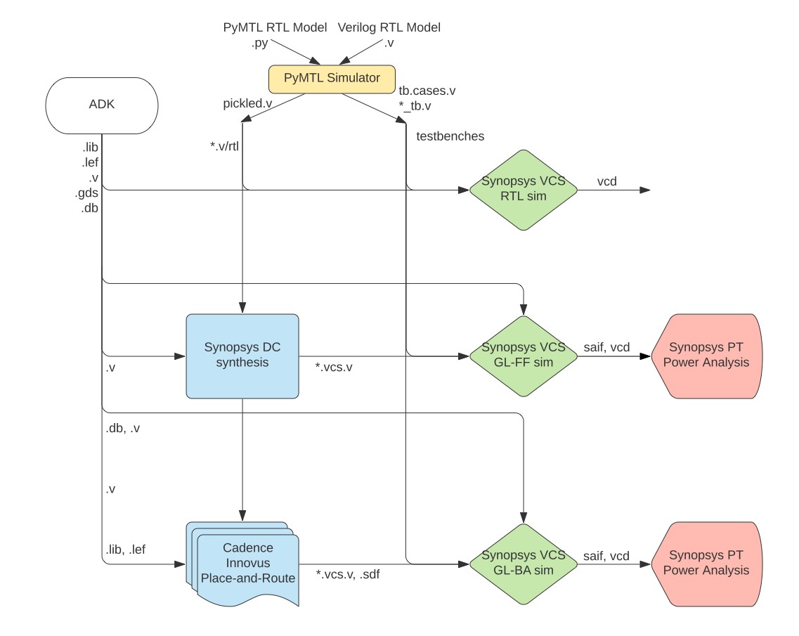
-
We use the PyMTL3 framework to test, verify, and evaluate the execution time (in cycles) of our design. This part of the flow is very similar to the flow used in ECE 4750. Note that we can write our RTL models in either PyMTL3 or Verilog, but we will always use PyMTL3 for the test harnesses, simulation drivers, and high-level modeling. Once we are sure our design is working correctly, we can then start to push the design through the flow. The ASIC flow requires Verilog RTL as an input, so we can use PyMTL3’s automatic translation tool to translate PyMTL3 RTL models into Verilog RTL.
-
We use Synopsys VCS to compile and run both 4-state RTL and gate-level simulations. These simulations help us to build confidence in our design as we push our designs through different stages of the flow. From these simulations, we also generate waveforms in
.vcd(Verilog Change Dump) format, and we usevcd2saifto convert these waveforms into per-net average activity factors stored in.saifformat. These activity factors will be used for power analysis. Gate-level simulation is an extremely valuable tool for ensuring the tools did not optimize something away which impacts the correctness of the design, and also provides an avenue for obtaining a more accurate power analysis than RTL simulation. Though Static Timing Analysis (STA) is much better because it analyzes all paths, GL simulation also serves as a backup to check for hold and setup time violations (chip designers must be paranoid!) -
We use Synopsys Design Compiler (DC) to synthesize our design, which means to transform the Verilog RTL model into a Verilog gate-level netlist where all of the gates are selected from the standard-cell library. We need to provide Synopsys DC with abstract logical and timing views of the standard-cell library in
.dbformat. In addition to the Verilog gate-level netlist, Synopsys DC can also generate a.ddcfile which contains information about the gate-level netlist and timing, and this.ddcfile can be inspected using Synopsys Design Vision (DV). -
We use Cadence Innovus to place-and-route our design, which means to place all of the gates in the gate-level netlist into rows on the chip and then to generate the metal wires that connect all of the gates together. We need to provide Cadence Innovus with the same abstract logical and timing views used in Synopsys DC, but we also need to provide Cadence Innovus with technology information in
.lef, and.captableformat and abstract physical views of the standard-cell library also in.lefformat. Cadence Innovus will generate an updated Verilog gate-level netlist, a.speffile which contains parasitic resistance/capacitance information about all nets in the design, and a.gdsfile which contains the final layout. The.gdsfile can be inspected using the open-source Klayout GDS viewer. Cadence Innovus also generates reports which can be used to accurately characterize area and timing. -
We use Synopsys PrimeTime (PT) to perform power analysis of our design. We need to provide Synopsys PT with the same abstract logical, timing, and power views used in Synopsys DC and Cadence Innovus, but in addition we need to provide switching activity information for every net in the design (which comes from the
.saiffile), and capacitance information for every net in the design (which comes from the.speffile). Synopsys PT puts the switching activity, capacitance, clock frequency, and voltage together to estimate the power consumption of every net and thus every module in the design, and these estimates are captured in various reports.
Extensive documentation is provided by Synopsys and Cadence for these ASIC tools. We have organized this documentation and made it available to you on the public course webpage. The username/password was distributed during lecture.
The first step is to source the setup script, clone this repository from GitHub, and define an environment variable to keep track of the top directory for the project.
% source setup-ece5745.sh
% mkdir -p $HOME/ece5745
% cd $HOME/ece5745
% git clone git@github.com:cornell-ece5745/ece5745-tut5-asic-tools
% cd ece5745-tut5-asic-tools
% TOPDIR=$PWD
Nangate 45nm Standard-Cell Library
Before you can gain access to a standard-cell library, you need to gain access to a “physical design kit” (PDK). A PDK includes all of the design files required for full-custom circuit design for a specific technology. So this will include a design-rule manual as well as SPICE circuit models for transistors and other devices. Gaining access to a real PDK is difficult. It requires negotiating with the foundry and signing multiple non-disclosure agreements. So in this course we will be using the FreePDK45 PDK:
- https://www.eda.ncsu.edu/wiki/FreePDK45
This is an open PDK for a “fake” technology. It was created by universities using publically available data on several different commercial 45nm processes. This means you cannot actually tapeout a chip using this PDK, but the technology is representative enough to provide reasonable area, energy, and timing estimates for research and teaching purposes. You can find the FreePDK45 PDK installed here:
% cd $ADK_PKGS/freepdk-45nm/pkgs/FreePDK45-1.4
A standard-cell designer will use the PDK to implement the standard-cell
library. A standard-cell library is a collection of combinational and
sequential logic gates that adhere to a standardized set of logical,
electrical, and physical policies. For example, all standard cells are
usually the same height, include pins that align to a predetermined
vertical and horizontal grid, include power/ground rails and nwells in
predetermined locations, and support a predetermined number of drive
strengths. A standard-cell designer will usually create a high-level
behavioral specification (in Verilog), circuit schematics (in SPICE), and
the actual layout (in .gds format) for each logic gate. The Synopsys
and Cadence tools do not actually use these low-level implementations,
since they are actually too detailed. Instead these tools use abstract
views of the standard cells, which capture logical functionality,
timing, geometry, and power usage at a much higher level.
Just like with a PDK, gaining access to a real standard-cell library is difficult. It requires gaining access to the PDK first, negotiating with a company which makes standard cells, and usually signing more non-disclosure agreements. In this course, we will be using the Nangate 45nm standard-cell library which is based on the open FreePDK45 PDK.
Nangate is a company which makes a tool to automatically generate standard-cell libraries, so they have made this library publically available a way to demonstrate their tool. Since it is an open library it is a great resource for research and teaching. Even though the standard-cell library is based on a “fake” 45nm PDK, the library provides a very reasonable estimate of a real commercial standard library in a real 45nm technology. In this section, we will take a look at both the low-level implementations and high-level views of the Nangate standard-cell library.
A standard-cell library distribution can contain gigabytes of data in thousands of files. For example, here is the distribution for the Nangate standard-cell library.
% cd $ADK_PKGS/freepdk-45nm/pkgs/NangateOpenCellLibrary_PDKv1_3_v2010_12
To simplify using the Nangate standard-cell library in this course, we have created a much smaller set of well-defined symlinks which point to just the key files we want to use in this course. We call this collection of symlinks an “ASIC design kit” (ADK). Here is the directory which contains these symlinks.
 % cd $ECE5745_STDCELLS
 % ls
 pdk-models.sp          # spice models for transistors

 rtk-stream-out.map     # gds layer map
 rtk-tech.lef           # interconnect technology information
 rtk-tech.tf            # interconnect technology information
 rtk-typical.captable   # interconnect technology information

 stdcells.spi           # circuit schematics for each cell
 stdcells.gds           # layout for each cell
 stdcells.v             # behavioral specification for each cell

 stdcells-lpe.spi       # circuit schematics with parasitics for each cell
 stdcells.lib           # abstract logical, timing, power view for each cell (typical)
 stdcells-bc.lib        # best case .lib
 stdcells-wc.lib        # worst case .lib
 stdcells.lef           # abstract physical view for each cell

 stdcells.db            # binary compiled version of .lib file
 stdcells.mwlib         # Milkyway database built from .lef file

 stdcells-databook.pdf  # standard-cell library databook

 klayout.lyp            # layer settings for Klayout
Let’s begin by looking at the schematic for a 3-input NAND cell (NAND3_X1).
 % less -p NAND3_X1 $ECE5745_STDCELLS/stdcells.spi
 .SUBCKT NAND3_X1 A1 A2 A3 ZN VDD VSS
 *.PININFO A1:I A2:I A3:I ZN:O VDD:P VSS:G
 *.EQN ZN=!((A1 * A2) * A3)
 M_i_2 net_1 A3 VSS   VSS NMOS_VTL W=0.415000U L=0.050000U
 M_i_1 net_0 A2 net_1 VSS NMOS_VTL W=0.415000U L=0.050000U
 M_i_0 ZN    A1 net_0 VSS NMOS_VTL W=0.415000U L=0.050000U
 M_i_5 ZN    A3 VDD   VDD PMOS_VTL W=0.630000U L=0.050000U
 M_i_4 VDD   A2 ZN    VDD PMOS_VTL W=0.630000U L=0.050000U
 M_i_3 ZN    A1 VDD   VDD PMOS_VTL W=0.630000U L=0.050000U
 .ENDS
For students with a circuits background, there should be no surprises
here, and for those students with less circuits background we will cover
basic static CMOS gate design later in the course. Essentially, this
schematic includes three NMOS transistors arranged in series in the
pull-down network, and three PMOS transistors arranged in parallel in the
pull-up network. The PMOS transistors are larger than the NMOS
transistors (see W= parameter) because the mobility of holes is less
than the mobility of electrons.
Now let’s look at the layout for the 3-input NAND cell using the open-source Klayout GDS viewer.
% klayout -l $ECE5745_STDCELLS/klayout.lyp $ECE5745_STDCELLS/stdcells.gds
Note that we are using the .lyp file which is a predefined layer color
scheme that makes it easier to view GDS files. To view the 3-input NAND
cell, find the NAND3X1 cell in the left-hand cell list, and then choose
_Display > Show as New Top from the menu. Here is a picture of the
layout for this cell.
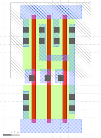
Diffusion is green, polysilicon is red, contacts are solid dark blue, metal 1 (M1) is blue, and the nwell is the large gray rectangle over the top half of the cell. All standard cells will be the same height and have the nwell in the same place. Notice the three NMOS transistors arranged in series in the pull-down network, and three PMOS transistors arranged in parallel in the pull-up network. The power rail is the horizontal strip of M1 at the top, and the ground rail is the horizontal strip of M1 at the bottom. All standard cells will have the power and ground rails in the same place so they will connect via abutment if these cells are arranged in a row. Although it is difficult to see, the three input pins and one output pin are labeled squares of M1, and these pins are arranged to be on a predetermined grid.
Now let’s look at the Verilog behavioral specification for the 3-input NAND cell.
 % less -p NAND3_X1 $ECE5745_STDCELLS/stdcells.v
 module NAND3_X1 (A1, A2, A3, ZN);
   input A1;
   input A2;
   input A3;
   output ZN;

   not(ZN, i_8);
   and(i_8, i_9, A3);
   and(i_9, A1, A2);

   specify
     (A1 => ZN) = (0.1, 0.1);
     (A2 => ZN) = (0.1, 0.1);
     (A3 => ZN) = (0.1, 0.1);
   endspecify

 endmodule
Note that the Verilog implementation of the 3-input NAND cell looks
nothing like the Verilog we used in ECE 4750. This cell is implemented
using Verilog primitive gates (e.g., not, and) and it includes a
specify block which is used for advanced gate-level simulation with
back-annotated delays.
We can use sophisticated tools to extract detailed parasitic resistance and capacitance values from the layout, and then we can add these parasitics to the circuit schematic to create a much more accurate model for experimenting with the circuit timing and power. Let’s look at a snippet of the extracted circuit for the 3-input NAND cell:
 % less -p NAND3_X1 $ECE5745_STDCELLS/stdcells-lpe.spi
 .SUBCKT NAND3_X1 VDD VSS A3 ZN A2 A1
 *.PININFO VDD:P VSS:G A3:I ZN:O A2:I A1:I
 *.EQN ZN=!((A1 * A2) * A3)
 M_M3 N_ZN_M0_d  N_A3_M0_g N_VDD_M0_s VDD PMOS_VTL W=0.630000U L=0.050000U
 M_M4 N_VDD_M1_d N_A2_M1_g N_ZN_M0_d  VDD PMOS_VTL W=0.630000U L=0.050000U
 M_M5 N_ZN_M2_d  N_A1_M2_g N_VDD_M1_d VDD PMOS_VTL W=0.630000U L=0.050000U
 M_M0 net_1      N_A3_M3_g N_VSS_M3_s VSS NMOS_VTL W=0.415000U L=0.050000U
 M_M1 net_0      N_A2_M4_g net_1      VSS NMOS_VTL W=0.415000U L=0.050000U
 M_M2 N_ZN_M5_d  N_A1_M5_g net_0      VSS NMOS_VTL W=0.415000U L=0.050000U
 C_x_PM_NAND3_X1%VDD_c0 x_PM_NAND3_X1%VDD_39 VSS 3.704e-17
 C_x_PM_NAND3_X1%VDD_c1 x_PM_NAND3_X1%VDD_36 VSS 2.74884e-18
 C_x_PM_NAND3_X1%VDD_c2 x_PM_NAND3_X1%VDD_26 VSS 2.61603e-16
 C_x_PM_NAND3_X1%VDD_c3 N_VDD_M1_d           VSS 6.57971e-17
 C_x_PM_NAND3_X1%VDD_c4 x_PM_NAND3_X1%VDD_19 VSS 1.89932e-17
 C_x_PM_NAND3_X1%VDD_c5 x_PM_NAND3_X1%VDD_18 VSS 3.74888e-17
 C_x_PM_NAND3_X1%VDD_c6 N_VDD_M0_s           VSS 3.64134e-17
 ...
 .ENDS
The full model is a couple of hundred lines long, so you can see how
detailed this model is! The ASIC tools do not really need this much
detail. We can use a special set of tools to create a much higher level
abstract view of the timing and power of this circuit suitable for use by
the ASIC tools. Essentially, these tools run many, many circuit-level
simulations to create characterization data stored in a .lib (Liberty)
file. Let’s look at snippet of the .lib file for the 3-input NAND cell.
 % less -p NAND3_X1 $ECE5745_STDCELLS/stdcells.lib
 cell (NAND3_X1) {
  drive_strength          : 1;
  area                    : 1.064000;
  cell_leakage_power      : 18.104768;
  leakage_power () {
    when                  : "!A1 & !A2 & !A3";
    value                 : 3.318854;
  }
  ...
  pin (A1) {
    direction             : input;
    related_power_pin     : "VDD";
    related_ground_pin    : "VSS";
    capacitance           : 1.590286;
    fall_capacitance      : 1.562033;
    rise_capacitance      : 1.590286;
  }
  ...
  pin (ZN) {
    direction             : output;
    related_power_pin     : "VDD";
    related_ground_pin    : "VSS";
    max_capacitance       : 58.364900;
    function              : "!((A1 & A2) & A3)";

    timing () {

      related_pin         : "A1";
      timing_sense        : negative_unate;

      cell_fall(Timing_7_7) {
        index_1 ("0.00117378,0.00472397,0.0171859,0.0409838,0.0780596,0.130081,0.198535");
        index_2 ("0.365616,1.823900,3.647810,7.295610,14.591200,29.182500,58.364900");
        values ("0.0106270,0.0150189,0.0204521,0.0312612,0.0528211,0.0959019,0.182032", \
                "0.0116171,0.0160692,0.0215549,0.0324213,0.0540285,0.0971429,0.183289", \
                "0.0157475,0.0207077,0.0261030,0.0369216,0.0585239,0.101654,0.187820", \
                "0.0193780,0.0263217,0.0337702,0.0462819,0.0677259,0.110616,0.196655", \
                "0.0218025,0.0305247,0.0399593,0.0560603,0.0822203,0.125293,0.210827", \
                "0.0229784,0.0334449,0.0447189,0.0640615,0.0959700,0.146382,0.231434", \
                "0.0227986,0.0349768,0.0480836,0.0705081,0.107693,0.167283,0.259623");
      }
      ...

      internal_power () {
        related_pin       : "A1";
        fall_power(Power_7_7) {
          index_1 ("0.00117378,0.00472397,0.0171859,0.0409838,0.0780596,0.130081,0.198535");
          index_2 ("0.365616,1.823900,3.647810,7.295610,14.591200,29.182500,58.364900");
          values ("0.523620,0.538965,0.551079,0.556548,0.561151,0.564018,0.564418", \
                  "0.459570,0.484698,0.509668,0.529672,0.543887,0.554682,0.559331", \
                  "0.434385,0.457202,0.470452,0.498312,0.517651,0.538469,0.550091", \
                  "0.728991,0.630651,0.581024,0.559124,0.551408,0.553714,0.557387", \
                  "1.306597,1.153240,1.010684,0.831268,0.727155,0.657699,0.616287", \
                  "2.170611,1.965158,1.760932,1.459438,1.140559,0.930355,0.781393", \
                  "3.276307,3.084566,2.831754,2.426623,1.913607,1.439055,1.113950");
        }
        ...
      }
  ...
 }
This is just a small subset of the information included in the .lib
file for this cell. We will talk more about the details of such .lib
files later in the course, but you can see that the .lib file contains
information about area, leakage power, capacitance of each input pin,
logical functionality, and timing. Units for all data is provided at the
top of the .lib file. In this snippet you can see that the area of the
cell is 1.064 square micron and the leakage power is 18.1nW. The
capacitance for the input pin A1 is 1.59fF, although there is
additional data that captures how the capacitance changes depending on
whether the input is rising or falling. The output pin ZN implements
the logic equation !((A1 & A2) & A3) (i.e., a three-input NAND gate).
Data within the .lib file is often represented using one- or
two-dimensional lookup tables (i.e., a values table). You can see two
such tables in the above snippet.
Let’s start by focusing on the first table. This table captures the delay
from input pin A1 to output pin ZN as a function of two parameters:
the input transition time (horizontal direction in lookup table) and the
load capacitance (vertical direction in lookup table). Note that this
delay is when ZN is “falling” (i.e., when it is transitioning from high
to low). There is another table for the delay when ZN is rising, and
there are additional tables for every input. Gates are slower when the
inputs take longer to transition and/or when they are driving large
output loads. Each entry in the lookup table reflects characterization of
one or more detailed circuit-level simulations. So in this example the
delay from input pin A1 to output pin ZN is 16ps when the input
transition rate is 4.7ps and the output load is 1.82fF. This level of
detail can enable very accurate static timing analysis of our designs.
Let’s now focus on the second table. This table captures the internal power, which is the power consumed within the gate itself, again as a function of two paramers: the input transition time (horizontal direction in lookup table) and the load capacitance (vertical direction in lookup table). Each entry in the lookup table is calculated by measuring the current drawn from the power supply during a detailed SPICE simulation and subtracting any current used to charge the output load. In other words all of the energy that is not consumed charging up the output load is considered internal energy. Note that sometimes the internal power is negative. This is simply due to how we account for energy. We can either assume all energy is consumed only when the output node is charged and no energy is consumed when the output node is discharged, or we can assume half the energy is consumed when the output is node is charged and half the energy is consumed when the output node is discharged in which case you will sometimes see negative internal power.
Note that some of the ASIC tools actually do not use the .lib file
directly, but instead use a pre-compiled binary version of the .lib
file stored in .db format. The binary .db file is usually much more
compact that the text .lib file. The .lib file captures the abstract
logical, timing, and power aspects of the standard-cell library, but it
does not capture the physical aspects of the standard-cell library. While
the ASIC tools could potentially use the .gds file directly, the ASIC
tools do not really need this much detail. We can use a special set of
tools to create a much higher level abstract view of the physical aspects
of the cell suitable for use by the ASIC tools. These tools create .lef
files. Let’s look at snippet of the the .lef file for the 3-input NAND
cell.
 % less -p NAND3_X1 $ECE5745_STDCELLS/stdcells.lef
MACRO NAND3_X1
  CLASS core ;
  FOREIGN NAND3_X1 0.0 0.0 ;
  ORIGIN 0 0 ;
  SYMMETRY X Y ;
  SITE FreePDK45_38x28_10R_NP_162NW_34O ;
  SIZE 0.76 BY 1.4 ;

  PIN A1
    DIRECTION INPUT ;
    ANTENNAPARTIALMETALAREA 0.0175 LAYER metal1 ;
    ANTENNAPARTIALMETALSIDEAREA 0.0715 LAYER metal1 ;
    ANTENNAGATEAREA 0.05225 ;
    PORT
      LAYER metal1 ;
        POLYGON 0.44 0.525 0.54 0.525 0.54 0.7 0.44 0.7  ;
    END
  END A1

  PIN ZN
    DIRECTION OUTPUT ;
    ANTENNAPARTIALMETALAREA 0.1352 LAYER metal1 ;
    ANTENNAPARTIALMETALSIDEAREA 0.4992 LAYER metal1 ;
    ANTENNADIFFAREA 0.197925 ;
    PORT
      LAYER metal1 ;
        POLYGON 0.235 0.8 0.605 0.8 0.605 0.15 0.675 0.15
         0.675 1.25 0.605 1.25 0.605 0.87 0.32 0.87 0.32 1.25 0.235 1.25  ;
    END
  END ZN

  PIN VDD
    DIRECTION INOUT ;
    USE power ;
    SHAPE ABUTMENT ;
    PORT
      LAYER metal1 ;
        POLYGON 0 1.315 0.04 1.315 0.04 0.975 0.11 0.975 0.11 1.315
         0.415 1.315 0.415 0.975 0.485 0.975 0.485 1.315 0.76 1.315 0.76 1.485 0 1.485  ;
    END
  END VDD

  ...
END NAND3_X1
This is just a small subset of the information included in the .lef
file for this cell. You can see the .lef file includes information on
the dimensions of the cell and the location and dimensions of both
power/ground and signal pins. The file also includes information on
“obstructions” (or blockages) indicated with a OBS entry. Take a look
at the NAND4_X4 gate to see an obstruction. These are regions of the cell
which should not be used by the ASIC tools. For example, if a cell needs
to use metal 2 (M2), it would create a blockage on M2 so that the ASIC
tools know not to route any M2 wires in that area. You can use Klayout to
view .lef files as well.
% klayout
Choose File > Import > LEF from the menu. Navigate to the
stdcells.lef file. Here is a picture of the .lef for this cell.
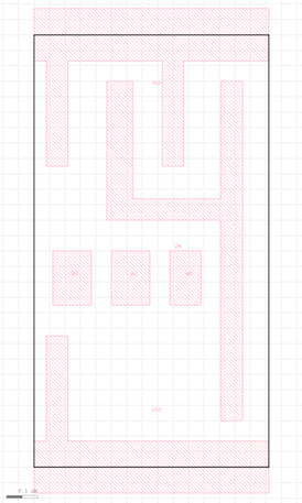
If you compare the .lef to the .gds you can see that the .lef is a
much simpler representation that only captures the boundary, pins, and
obstructions.
The standard-cell library also includes several files (e.g.,
rtk-tech.tf, rtk-tech.lef, rtk-typical.captable) that capture
information about the metal interconnect including the wire width, pitch,
and parasitics. For example, let’s take a look at the .captable file:
 % less -p M1 $ECE5745_STDCELLS/rtk-typical.captable
 LAYER M1
   MinWidth              0.07000
   MinSpace              0.06500
#  Height                0.37000
   Thickness             0.13000
   TopWidth              0.07000
   BottomWidth           0.07000
   WidthDev              0.00000
   Resistance            0.38000
 END
 ...
 M1
 width(um)  space(um) Ctot(Ff/um)  Cc(Ff/um)    Carea(Ff/um) Cfrg(Ff/um)
 0.070       0.052       0.1986       0.0723       0.0311       0.0115
 0.070       0.065       0.1705       0.0509       0.0311       0.0143
 0.070       0.200       0.1179       0.0115       0.0311       0.0319
 0.070       0.335       0.1150       0.0030       0.0311       0.0388
 0.070       0.470       0.1148       0.0009       0.0311       0.0409
 0.070       0.605       0.1147       0.0002       0.0311       0.0416
 0.070       0.740       0.1147       0.0001       0.0311       0.0417
This file contains information about the minimum dimenisions of wires on M1 and the resistance of these wires. It also contains a table of wire capacitances with different rows for different wire widths and spacings. The ASIC tools can use this kind of technology information to optimize and analyze the design.
Finally, a standard-cell library will always include a databook, which is a document that describes the details of every cell in the library. Take a few minutes to browse through the Nangate standard-cell library databook located on the class Canvas page here:
- https://canvas.cornell.edu/files/3153288/download
PyMTL3-Based Testing, Simulation, Translation
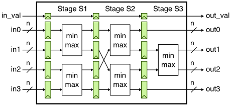
Our goal in this tutorial is to generate layout for the sort unit from the PyMTL3 tutorial using the ASIC tools. As a reminder, the sort unit takes as input four integers and a valid bit and outputs those same four integers in increasing order with the valid bit. The sort unit is implemented using a three-stage pipelined, bitonic sorting network and the datapath is shown below.
Let’s start by running the tests for the sort unit and note that the
tests for the SortUnitStructRTL will fail.
 % mkdir -p $TOPDIR/sim/build
 % cd $TOPDIR/sim/build
 % pytest ../tut3_pymtl/sort
 % pytest ../tut3_pymtl/sort --test-verilog --dump-vtb
You can just copy over your implementation of the MinMaxUnit from when
you completed the PyMTL3 tutorial. If you have not completed the PyMTL3
tutorial then you might want to go back and do that now. Basically the
MinMaxUnit should look like this:
from pymtl3 import *

class MinMaxUnit( Component ):

  # Constructor

  def construct( s, nbits ):

    s.in0     = InPort ( nbits )
    s.in1     = InPort ( nbits )
    s.out_min = OutPort( nbits )
    s.out_max = OutPort( nbits )

    @update
    def block():

      if s.in0 >= s.in1:
        s.out_max @= s.in0
        s.out_min @= s.in1
      else:
        s.out_max @= s.in1
        s.out_min @= s.in0

  # Line tracing

  def line_trace( s ):
    return f"{s.in0}|{s.in1}(){s.out_min}|{s.out_max}"
The --test-verilog command line option tells the PyMTL3 framework to
first translate the sort unit into Verilog, and then import it back
into PyMTL3 to verify that the translated Verilog is itself correct. With
the --test-verilog command line option, PyMTL3 will skip tests that are
not for verifying RTL. The dump_vtb command line option tells PyMTL3 to
dump the Verilog Testbench. While we can do RTL simulation using Python,
we need to translate our testbenches to Verilog so that we can use
Synopsys VCS to do 4-state and gate-level simulation. Let’s look at a
testbench cases file generated from using the --dump-vtb flag.
 % cd $TOPDIR/sim/build
 % cat SortUnitStructRTL__nbits_8_test_basic_tb.v.cases

  `T('h00,'h00,'h00,'h00,'h0,'h00,'h00,'h00,'h00,'h0);
  `T('h04,'h02,'h03,'h01,'h1,'h00,'h00,'h00,'h00,'h0);
  `T('h00,'h00,'h00,'h00,'h0,'h00,'h00,'h00,'h00,'h0);
  `T('h00,'h00,'h00,'h00,'h0,'h00,'h00,'h00,'h00,'h0);
  `T('h00,'h00,'h00,'h00,'h0,'h01,'h02,'h03,'h04,'h1);
  `T('h00,'h00,'h00,'h00,'h0,'h00,'h00,'h00,'h00,'h0);
  `T('h00,'h00,'h00,'h00,'h0,'h00,'h00,'h00,'h00,'h0);
  `T('h00,'h00,'h00,'h00,'h0,'h00,'h00,'h00,'h00,'h0);
  `T('h00,'h00,'h00,'h00,'h0,'h00,'h00,'h00,'h00,'h0);
This file is generated by logging the inputs and outputs of your PyMTL3 RTL simulation each cycle, and it will be passed into a Verilog testbench runner that will use these values to set the inputs each cycle, and to verify the outputs each cycle. So note that when we utilize these testbenches later on, we are running a simulation that is simply confirming that we acheive the same behavior as the RTL simulation we run in PyMTL3, and it is not actually using any assertions you wrote in your Python tests for your design. Therefore, it is important that your RTL simulations pass in PyMTL3 before you move on to other simulations. Also take a look at the testbench itself to get a sense for how it works. It essentially instantiates your top module as ‘DUT’, sets the inputs, and performs a check every cycle on the outputs.
% less SortUnitStructRTL__nbits_8_test_basic_tb.v
After running the tests we use the sort unit simulator to do the final
translation into Verilog and to dump the vtb file that will allow us
to do 4-state RTL simulation using Synopsys VCS.
 % cd $TOPDIR/sim/build
 % ../tut3_pymtl/sort/sort-sim --impl rtl-struct --stats --translate --dump-vtb
 num_cycles          = 106
 num_cycles_per_sort = 1.06
Take a moment to open up the translated Verilog which should be in a file
named SortUnitStructRTL__nbits_8__pickled.v. Try to see how both the structural
composition and the behavioral modeling translates into Verilog. Here is
an example of the translation for the MinMaxUnit. Notice how PyMTL3 will
output the source Python embedded as a comment in the corresponding
translated Verilog.
 % cd $TOPDIR/sim/build
 % less SortUnitStructRTL__nbits_8__pickled.v

 // PyMTL Component MinMaxUnit Definition
 // At .../sim/tut3_pymtl/sort/MinMaxUnit.py
 module MinMaxUnit__nbits_8
 (
   input  logic [0:0] clk,
   input  logic [7:0] in0,
   input  logic [7:0] in1,
   output logic [7:0] out_max,
   output logic [7:0] out_min,
   input  logic [0:0] reset
 );

    // PyMTL Update Block Source
    // At /home/sj634/workspace/ece5745-labs/sim/tut3_pymtl/sort/MinMaxUnit.py:26
    // @update
    // def block():
    //
    //   if s.in0 >= s.in1:
    //     s.out_max @= s.in0
    //     s.out_min @= s.in1
    //   else:
    //     s.out_max @= s.in1
    //     s.out_min @= s.in0

   always_comb begin : block
     if ( in0 >= in1 ) begin
       out_max = in0;
       out_min = in1;
     end
     else begin
       out_max = in1;
       out_min = in0;
     end
   end

 endmodule
The Verilog module name includes a suffix to make it unique for a specific set of parameters. Although we hope students will not need to actually open up this translated Verilog it is occasionally necessary. For example, PyMTL3 is not perfect and can translate incorrectly which might require looking at the Verilog to see where it went wrong. Other steps in the ASIC flow might refer to an error in the translated Verilog which will also require looking at the Verilog to figure out why the other steps are going wrong. While we try and make things as automated as possible, students will eventually need to dig in and debug some of these steps themselves.
Using Synopsys VCS for 4-state RTL simulation
Using the PyMTL simulation framework can give us a good foundation in
verifying a design. However, the PyMTL RTL simulation that you may be
accustomed to in ECE 4750 is only a 2-state simulation, meaning a signal
can only be 0 or 1. An alternative form of RTL simulation is a
4-state simulation, in which signals can be 0, 1, x, or z.
It is important to note a key difference between 2-state and 4-state
simulation. In 2-state simulation, each variable is initialized to a
determined value. This initial condition assumption may or may not be
what happens in actual silicon! As a result, a different initial condition
could introduce a bug that was not caught by our PyMTL3 2-state RTL
simulation. In 4-state simulations no such assumptions are made. Instead,
every signal begins as x, and only resolves to a 0 or 1 after it
is driven or resolved using x-propagation.
always @(*)
begin
  if ( control_signal )
    // set signal "signal_a", but bug causes chip to fail
  else
    // set signal "signal_a" such that everything works fine
end
Look at the above pseudocode. If control_signal is not reset, then in
2-state simulation if you initialize all state to zero it will look like
the chip works fine, but this is not a safe assumption! The real chip
does not guarantee that all state is initialized to zero, so we can model
that in four state simulation as an x. Since the control signal could
initialize to 1, this could non-deterministically cause the chip to fail!
What you would see in simulation is that signal_a would become an x,
because we do not know the value of control_signal on reset. This x is
propogated through the design, and some simulators are more optimistic/pessimistic
about x’s than others. For example, a pessimistic simulator may just assume
that any piece of logic that has an x on the input, outputs an x. This is
pessimistic because it is possible that you can still resolve the output
(imagine a mux where two inputs are the same but the select bit is an x).
Optimism is the opposite, resolving signals to 0 or 1 that
should remain an x.
You may notice in your designs that you are passing all 2-state simulations,
but fail every 4-state simulation. Oftentimes the key to this is that an
output is an x for some cycle, which is a good sign you are not handling
reset properly. We consider it best practice to force invalid output data
to zero, to avoid x’s in your 4-state simulation, and provide a
deterministic output for every cycle no matter the initial condition.
To create a 4-state simulation, let’s start by creating another build directory for our vcs work.
% mkdir -p $TOPDIR/asic-manual/vcs-rtl-build
% cd $TOPDIR/asic-manual/vcs-rtl-build
We run vcs to compile a simulation, and ./simv to run the simulation.
Let’s run a 4-state simulation for test_basic using the design
SortUnitStructRTL__nbits_8__pickled.v.
% vcs ../../sim/build/SortUnitStructRTL__nbits_8__pickled.v -full64 -sverilog +incdir+../../sim/build +lint=all -xprop=tmerge -top SortUnitStructRTL__nbits_8_tb ../../sim/build/SortUnitStructRTL__nbits_8_test_basic_tb.v +vcs+dumpvars+SortUnitStructRTL__nbits_8_test_basic_vcs.vcd -override_timescale=1ns/1ns
% ./simv
Synopsys VCS is an extremely in-depth tool with many command line options. If you want to learn more on your own about other options that are available to you with VCS, you can visit the course webpage here. However, we’ve detailed some of the key command line options below:
../../sim/build/SortUnitStructRTL__nbits_8__pickled.v        -The path to the source RTL file
-sverilog                                             -Indicates that we are using SystemVerilog
+incdir+../../sim/build                                      -Specifies directories that contain files that are tagged with `include. We include ../../sim/build because our VTB
                                                       includes a _tb.v.cases file located within the ../../sim/build directory
-xprop=tmerge                                         -Specifies that we want to use the tmerge truth table for x-propagation (see VCS user manual for more info)
-top SortUnitStructRTL__nbits_8_tb                    -Indicates the name of the top module (located within the VTB)
../../sim/build/SortUnitStructRTL__nbits_8_test_basic_tb.v   -The path to the source testbench file
+define+<macro>                                       -defines a macro that may be used in your verilog code or testbench
+vcs+dumpvars+<filename>.vcd                          -Tells VCS to dump a VCD in the current dir with the name <filename>.vcd
-override_timescale=1ns/1ns                           -Changes the timescale. Units/precision
Let’s run another 4-state simulation, this time using the testbench from the sort-rtl simulator run that we ran earlier. Note that while we can use this vcd for power analysis, for the purposes of this tutorial we will only be doing power analysis on the final gate-level netlist that we’ll obtain from Cadence Innovus.
% vcs ../../sim/build/SortUnitStructRTL__nbits_8__pickled.v -full64 -sverilog +incdir+../../sim/build +lint=all -xprop=tmerge -top SortUnitStructRTL__nbits_8_tb ../../sim/build/SortUnitStructRTL__nbits_8_sort-rtl-struct-random_tb.v +vcs+dumpvars+SortUnitStructRTL__nbits_8_sort-rtl-struct-random_vcs.vcd -override_timescale=1ns/1ns
% ./simv
Using Synopsys Design Compiler for Synthesis
We use Synopsys Design Compiler (DC) to synthesize Verilog RTL models
into a gate-level netlist where all of the gates are from the standard
cell library. So Synopsys DC will synthesize the Verilog + operator
into a specific arithmetic block at the gate-level. Based on various
constraints it may synthesize a ripple-carry adder, a carry-look-ahead
adder, or even more advanced parallel-prefix adders.
We start by creating a subdirectory for our work, and then launching Synopsys DC.
 % mkdir -p $TOPDIR/asic-manual/synopsys-dc
 % cd $TOPDIR/asic-manual/synopsys-dc
 % dc_shell-xg-t
To make it easier to copy-and-paste commands from this document, we tell
Synopsys DC to ignore the prefix dc_shell> using the following:
dc_shell> alias "dc_shell>" ""
There are two important variables we need to set before starting to work
in Synopsys DC. The target_library variable specifies the standard
cells that Synopsys DC should use when synthesizing the RTL. The
link_library variable should search the standard cells, but can also
search other cells (e.g., SRAMs) when trying to resolve references in our
design. These other cells are not meant to be available for Synopsys DC
to use during synthesis, but should be used when resolving references.
Including * in the link_library variable indicates that Synopsys DC
should also search all cells inside the design itself when resolving
references.
 dc_shell> set_app_var target_library "$env(ECE5745_STDCELLS)/stdcells.db"
 dc_shell> set_app_var link_library   "* $env(ECE5745_STDCELLS)/stdcells.db"
Note that we can use $env(ECE5745_STDCELLS) to get access to the
$ECE5745_STDCELLS environment variable which specifies the directory
containing the standard cells, and that we are referencing the abstract
logical and timing views in the .db format.
As an aside, if you want to learn more about any command in any Synopsys
tool, you can simply type man toolname at the shell prompt. We are now
ready to read in the Verilog file which contains the top-level design and
all referenced modules. We do this with two commands. The analyze
command reads the Verilog RTL into an intermediate internal
representation. The elaborate command recursively resolves all of the
module references starting from the top-level module, and also infers
various registers and/or advanced data-path components.
 dc_shell> analyze -format sverilog ../../sim/build/SortUnitStructRTL__nbits_8__pickled.v
 dc_shell> elaborate SortUnitStructRTL__nbits_8
We need to create a clock constraint to tell Synopsys DC what our target
cycle time is. Synopsys DC will not synthesize a design to run “as fast
as possible”. Instead, the designer gives Synopsys DC a target cycle time
and the tool will try to meet this constraint while minimizing area and
power. The create_clock command takes the name of the clock signal in
the Verilog (which in this course will always be clk), the label to
give this clock (i.e., ideal_clock1), and the target clock period in
nanoseconds. So in this example, we are asking Synopsys DC to see if it
can synthesize the design to run at 3.33GHz (i.e., a cycle time of 300ps).
dc_shell> create_clock clk -name ideal_clock1 -period 0.3
In an ideal world, all inputs and outputs would change immediately with the clock edge. In reality, this is not the case. We need to include reasonable delays for inputs and outputs, so Synopsys DC can factor this into its timing analysis so we would still meet timing if we were to tape our design out in real silicon. Here, we choose 5% of the clock period for our input and output delays.
 dc_shell> set_input_delay -clock ideal_clock1 [expr 0.3*0.05] [all_inputs]
 dc_shell> set_output_delay -clock ideal_clock1 [expr 0.3*0.05] [all_outputs]
Next, we give Synopsys DC some constraints about fanout and transition slew. Fanout roughly describes the number of inputs driven by a particular output, and the higher the fanout, the higher the drive strength required. Slew rate is how quickly a signal can make a full transition. We want all of our signals to meet a good slew, meaning that they can transition quickly, so we set maximum slew to one quarter of the clock period.
 dc_shell> set_max_fanout 20 SortUnitStructRTL__nbits_8
 dc_shell> set_max_transition [expr 0.25*0.3] SortUnitStructRTL__nbits_8
We can use the check_design command to make sure there are no obvious
errors in our Verilog RTL.
dc_shell> check_design
You may see some warnings regarding clk[0] and reset[0] ports not
being connected to any nets in certain modules. This is ok, since in
PyMTL translation we automatically add those ports to all modules, so
they may not actually be used. Aside from this, you should not see any
warnings. However, it is critical that you carefully review all
warnings and errors when you analyze and elaborate a design with Synopsys
DC. There may be many warnings, but you should still skim through them.
Often times there will be something very wrong in your Verilog RTL which
means any results from using the ASIC tools is completely bogus. Synopsys
DC will output a warning, but Synopsys DC will usually just keep going,
potentially producing a completely incorrect gate-level model!
Finally, the compile command will do the synthesis.
dc_shell> compile
During synthesis, Synopsys DC will display information about its optimization process. It will report on its attempts to map the RTL into standard-cells, optimize the resulting gate-level netlist to improve the delay, and then optimize the final design to save area.
The compile command does not flatten your design. Flatten means to
remove module hierarchy boundaries; so instead of having module A and
module B within module C, Synopsys DC will take all of the logic in
module A and module B and put it directly in module C. You can enable
flattening with the -ungroup_all option. Without extra hierarchy
boundaries, Synopsys DC is able to perform more optimizations and
potentially achieve better area, energy, and timing. However, an
unflattened design is much easier to analyze, since if there is a module
A in your RTL design that same module will always be in the synthesized
gate-level netlist.
The compile command does not perform many optimizations. Synopsys DC
also includes compile_ultra which does many more optimizations and will
likely produce higher quality of results. Keep in mind that the compile
command will not flatten your design by default, while the
compile_ultra command will flattened your design by default. You can
turn off flattening by using the -no_autoungroup option with the
compile_ultra command. compile_ultra also has the option -gate_clock
which automatically performs clock gating on your design, which can save
quite a bit of power. Once you finish this tutorial, feel free to go
back and experiment with the compile_ultra command.
Now that we have synthesized the design, we output the resulting
gate-level netlist in two different file formats: Verilog and .ddc
(which we will use with Synopsys DesignVision). We also output an
.sdc file which contains the constraint information we gave synopsys.
We will pass this same constraint information to cadence innovus during
the place and route portion of the flow.
 dc_shell> write -format verilog -hierarchy -output post-synth.v
 dc_shell> write -format ddc     -hierarchy -output post-synth.ddc
 dc_shell> write_sdc -nosplit post-synth.sdc
We can use various commands to generate reports about area, energy, and
timing. The report_timing command will show the critical path through
the design. Part of the report is displayed below. Note that this report
was generated using a clock constraint of 300ps.
 dc_shell> report_timing -nosplit -transition_time -nets -attributes
  ...
  Point                                       Fanout     Trans  Incr  Path
  --------------------------------------------------------------------------
  clock ideal_clock1 (rise edge)                                0.00  0.00
  clock network delay (ideal)                                   0.00  0.00
  elm_S0S1__0/out_reg[5]/CK (DFF_X1)                      0.00  0.00  0.00 r
  elm_S0S1__0/out_reg[5]/Q (DFF_X1)                       0.01  0.09  0.09 r
  elm_S0S1__0/out[5] (net)                      2               0.00  0.09 r
  elm_S0S1__0/out[5] (Reg__Type_Bits8_0)                        0.00  0.09 r
  elm_S0S1__out[5] (net)                                        0.00  0.09 r
  minmax0_S1/in0[5] (MinMaxUnit__DataType_Bits8_0)              0.00  0.09 r
  minmax0_S1/in0[5] (net)                                       0.00  0.09 r
  minmax0_S1/U56/ZN (INV_X1)                              0.01  0.03  0.12 f
  minmax0_S1/n64 (net)                          3               0.00  0.12 f
  minmax0_S1/U44/ZN (NAND2_X1)                            0.01  0.03  0.14 r
  minmax0_S1/n43 (net)                          1               0.00  0.14 r
  minmax0_S1/U40/ZN (OAI21_X1)                            0.01  0.03  0.18 f
  minmax0_S1/n44 (net)                          2               0.00  0.18 f
  minmax0_S1/U47/ZN (NOR2_X1)                             0.02  0.04  0.22 r
  minmax0_S1/n45 (net)                          1               0.00  0.22 r
  minmax0_S1/U13/ZN (OAI221_X1)                           0.02  0.05  0.27 f
  minmax0_S1/n10 (net)                          2               0.00  0.27 f
  minmax0_S1/U49/ZN (NAND2_X1)                            0.03  0.06  0.33 r
  minmax0_S1/n59 (net)                          6               0.00  0.33 r
  minmax0_S1/U69/ZN (OAI22_X1)                            0.01  0.04  0.38 f
  minmax0_S1/out_min[3] (net)                   1               0.00  0.38 f
  minmax0_S1/out_min[3] (MinMaxUnit__DataType_Bits8_0)          0.00  0.38 f
  minmax0_S1__out_min[3] (net)                                  0.00  0.38 f
  elm_S1S2__0/in_[3] (Reg__Type_Bits8_8)                        0.00  0.38 f
  elm_S1S2__0/in_[3] (net)                                      0.00  0.38 f
  elm_S1S2__0/out_reg[3]/D (DFF_X1)                       0.01  0.01  0.38 f
  data arrival time                                                   0.38

  clock ideal_clock1 (rise edge)                                0.30  0.30
  clock network delay (ideal)                                   0.00  0.30
  elm_S1S2__0/out_reg[3]/CK (DFF_X1)                            0.00  0.30 r
  library setup time                                           -0.04  0.26
  data required time                                                  0.26
  --------------------------------------------------------------------------
  data required time                                                  0.26
  data arrival time                                                  -0.38
  --------------------------------------------------------------------------
  slack (VIOLATED)                                                   -0.13
This timing report uses static timing analysis to find the critical
path. Static timing analysis checks the timing across all paths in the
design (regardless of whether these paths can actually be used in
practice) and finds the longest path. For more information about static
timing analysis, consult Chapter 1 of the Synopsys Timing Constraints
and Optimization User
Guide. The
report clearly shows that the critical path starts at bit 5 of a pipeline
register in between the S1 and S2 stages (elm_S0S1__0), goes into the
first input of a MinMaxUnit, comes out the out_min port of the
MinMaxUnit, and ends at a pipeline register in between the S1 and S2
stages (elm_S1S2__0). The report shows the delay through each logic
gate (e.g., the clk-to-q delay of the initial DFF is 90ps, the
propagation delay of a NAND2_X1 gate is 30ps) and the total delay for the
critical path which in this case is 0.38ns. Notice that there are two
NAND2_X1 gates, but they do have the same propagation delay; this is
because the static timing analysis also factors in input slew rates, rise
vs fall time, and output load when calculating the delay of each gate. We
set the clock constraint to be 300ps, but also notice that the report
factors in the setup time required at the final register. The setup time
is 40ps, so in order to operate the sort unit at 1ns and meet the setup
time we would need the critical path to arrive in 260ps.
The difference between the required arrival time and the actual arrival time is called the slack. Positive slack means the path arrived before it needed to while negative slack means the path arrived after it needed to. If you end up with negative slack, then you need to rerun the tools with a longer target clock period until you can meet timing with no negative slack. The process of tuning a design to ensure it meets timing is called “timing closure”. In this course we are primarily interested in design-space exploration as opposed to meeting some externally defined target timing specification. So you will need to sweep a range of target clock periods. Your goal is to choose the shortest possible clock period which still meets timing without any negative slack! This will result in a well-optimized design and help identify the “fundamental” performance of the design. Alternatively, if you are comparing multiple designs, sometimes the best situation is to tune the baseline so it has a couple of percent of negative slack and then ensure the alternative designs have similar cycle times. This will enable a fair comparison since all designs will be running at the same cycle time.
The report_area command can show how much area each module uses and can
enable detailed area breakdown analysis.
 dc_shell> report_area -nosplit -hierarchy
 ...
 Combinational area:         339.682001
 Buf/Inv area:                90.440000
 Noncombinational area:      451.401984
 Macro/Black Box area:         0.000000
 Net Interconnect area:       undefined  (Wire load has zero net area)

 Total cell area:            791.083986
 Total area:                  undefined

 Hierarchical area distribution
 ------------------------------

                    Global      Local
                    Cell Area   Cell Area
                    ----------  ----------------
 Hierarchical cell  Abs               Non  Black
                    Total  %    Comb  Comb Boxes
 ----------------- ------ ---- ----- ----- ---  -------------------------------
 SortUnitStructRTL  791.0  100   0.0   0.0 0.0  SortUnitStructRTL__8bit
 elm_S0S1__0         36.1  4.6   0.0  36.1 0.0  Reg__Type_Bits8_0
 elm_S0S1__1         36.1  4.6   0.0  36.1 0.0  Reg__Type_Bits8_11
 elm_S0S1__2         36.1  4.6   0.0  36.1 0.0  Reg__Type_Bits8_10
 elm_S0S1__3         36.1  4.6   0.0  36.1 0.0  Reg__Type_Bits8_9
 elm_S1S2__0         36.1  4.6   0.0  36.1 0.0  Reg__Type_Bits8_8
 elm_S1S2__1         36.1  4.6   0.0  36.1 0.0  Reg__Type_Bits8_7
 elm_S1S2__2         36.1  4.6   0.0  36.1 0.0  Reg__Type_Bits8_6
 elm_S1S2__3         36.1  4.6   0.0  36.1 0.0  Reg__Type_Bits8_5
 elm_S2S3__0         36.7  4.6   0.0  36.7 0.0  Reg__Type_Bits8_4
 elm_S2S3__1         37.2  4.7   0.0  37.2 0.0  Reg__Type_Bits8_3
 elm_S2S3__2         37.7  4.8   0.0  37.7 0.0  Reg__Type_Bits8_2
 elm_S2S3__3         36.7  4.6   0.0  36.7 0.0  Reg__Type_Bits8_1
 minmax0_S1          75.5  9.5  75.5   0.0 0.0  MinMaxUnit__DataType_Bits8_0
 minmax0_S2          72.6  9.2  72.6   0.0 0.0  MinMaxUnit__DataType_Bits8_4
 minmax1_S1          71.2  9.0  71.2   0.0 0.0  MinMaxUnit__DataType_Bits8_3
 minmax1_S2          72.3  9.1  72.3   0.0 0.0  MinMaxUnit__DataType_Bits8_2
 minmax_S3           43.8  5.5  43.8   0.0 0.0  MinMaxUnit__DataType_Bits8_1
 val_S0S1             5.8  0.7   1.3   4.5 0.0  RegRst__Type_Bits1__reset_value_0_0
 val_S1S2             5.8  0.7   1.3   4.5 0.0  RegRst__Type_Bits1__reset_value_0_2
 val_S2S3             5.8  0.7   1.3   4.5 0.0  RegRst__Type_Bits1__reset_value_0_1
 ----------------- ------ ---- ----- ----- ---  -------------------------------
 Total                         339.6 451.4 0.0
The units are in square micron. The cell area can sometimes be different
from the total area. The total cell area includes just the standard
cells, while the total area can include interconnect area as well. If
available, we will want to use the total area in our analysis. Otherwise
we can just use the cell area. So we can see that the sort unit consumes
approximately 791um^2 of area. We can also see that each pipeline
register consumes about 4-5% of the area, while the MinMaxUnits consume
about ~40% of the area. This is one reason we try not to flatten our
designs, since the module hierarchy helps us understand the area
breakdowns. If we completely flattened the design there would only be one
line in the above table.
The report_power command can show how much power each module consumes.
Note that this power analysis is actually not that useful yet, since at
this stage of the flow the power analysis is based purely on statistical
activity factor estimation. Basically, Synopsys DC assumes every net
toggles 10% of the time. This is a pretty poor estimate, so we should
never use this kind of statistical power estimation in this course.
dc_shell> report_power -nosplit -hierarchy
Finally, we go ahead and exit Synopsys DC.
dc_shell> exit
Take a few minutes to examine the resulting Verilog gate-level netlist.
Notice that the module hierarchy is preserved and also notice that the
MinMaxUnit synthesizes into a large number of basic logic gates.
 % cd $TOPDIR/asic-manual/synopsys-dc
 % more post-synth.v
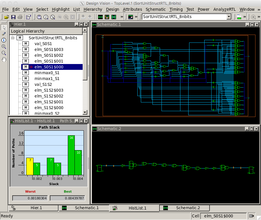
We can use the Synopsys Design Vision (DV) tool for browsing the
resulting gate-level netlist, plotting critical path histograms, and
generally analyzing our design. Start Synopsys DV and setup the
target_library and link_library variables as before.
 % cd $TOPDIR/asic-manual/synopsys-dc
 % design_vision-xg
 design_vision> set_app_var target_library "$env(ECE5745_STDCELLS)/stdcells.db"
 design_vision> set_app_var link_library   "* $env(ECE5745_STDCELLS)/stdcells.db"
Choose File > Read from the menu to open post-synth.ddc file
generated during synthesis. You can then use the following steps to view
the gate-level schematic for the MinMaxUnit:
- Select the
minmax0_S1module in the Logical Hierarchy panel - Choose Schematic > New Schematic View from the menu
- Double click the box representing the
MinMaxUnitin the schematic view
This shows you the exact gates used to implement the MinMaxUnit. You
can use the following steps to view a histogram of path slack, and also
to open a gave-level schematic of just the critical path.
- Choose Timing > Path Slack from the menu
- Click OK in the pop-up window
- Select the left-most bar in the histogram to see list of most critical paths
- Right click first path (the critical path) and choose Path Schematic
This shows you the exact gates that lie on the critical path. Notice that there nine levels of logic (including the registers) on the critical path. The number of levels of logic on the critical path can provide some very rough first-order intuition on whether or not we might want to explore a more aggressive clock constraint and/or adding more pipeline stages. If there are just a few levels of logic on the critical path then our design is probably very simple (as in this case!), while if there are more than 50 levels of logic then there is potentially room for signficant improvement. The following screen capture illutrates using Design Vision to explore the post-synthesis results. While this can be interesting, in this course, we almost always prefer exploring the post-place-and-route results, so we will not really use Synopsys DC that often.
To Do On Your Own: Sweep a range of target clock frequencies to
determine the shortest possible clock period which still meets timing
without any negative slack. You can put a sequence of commands in a
.tcl file and then run Synopsys DC using those commands in one step
like this:
 % cd $TOPDIR/asic-manual/synopsys-dc
 % dc_shell-xg-t -f init.tcl
So consider placing the commands from this section into a .tcl file
and then running Synopsys DC with a target clock period of 0.3ns. Then
gradually increase the clock period until your design meets timing. To
follow along with the tutorial, push the design through synth again using 0.6
ns as your clock constraint, as this is what we will be using for the
rest of the flow.
Using Synopsys VCS for Fast Functional Gate-Level Simulation
Before synthesis, we used Synopsys VCS to do a 4-state simulation. This time, we’ll be using VCS to perform a gate-level simulation, since we now have a gate-level netlist available to us. Gate-level simulation provides an advantage over RTL simulation because it more precisely represents the specification of the true hardware generated by the tools. This sort of simulation could propogate X’s into the design that were not found by the 4-state RTL simulation, and it also verifies that the tools did not optimize anything away during synthesis. A fast-functional simulation is a zero delay simulation which provides a way to check functionality at the gate level without worrying about the timing checks involved in a back-annotated gate-level simulation, which we’ll perfrom later in this tutorial.
We’ll start by creating a build directory for our post-synth run of vcs.
% mkdir -p $TOPDIR/asic-manual/vcs-postsyn-build
% cd $TOPDIR/asic-manual/vcs-postsyn-build
Then we’ll run vcs and ./simv to run our gate-level simulation on the sort-rtl-struct-random simulator testbench:
% vcs ../synopsys-dc/post-synth.v $ECE5745_STDCELLS/stdcells.v -full64 -sverilog +incdir+../../sim/build +lint=all -xprop=tmerge -top SortUnitStructRTL__nbits_8_tb ../../sim/build/SortUnitStructRTL__nbits_8_sort-rtl-struct-random_tb.v +define+CYCLE_TIME=0.6 +define+VTB_INPUT_DELAY=0.03 +define+VTB_OUTPUT_ASSERT_DELAY=0.57 +delay_mode_zero +vcs+dumpvars+SortUnitStructRTL__nbits_8_sort-rtl-struct-random_vcs.vcd -override_timescale=1ns/1ps
% ./simv
Notice there are some differences in the vcs command we ran here, and the
one we ran for 4-state RTL simulation. In this version, we use the
gate-level netlist post-synth.v instead of the pickled file. We also include
the option +delay_mode_zero which tells vcs to run a fast-functional simulation
in which no delays are considered. This is similar to RTL simulation, and you
should notice that all signals will change on the clock edge. We also include the
macros CYCLE_TIME, VTB_INPUT_DELAY , VTB_OUTPUT_ASSERT_DELAY. These values
are not actually critical for a fast-functional simulation, but we set them to the
same values as the Back-Annotated gate-level simulations to make comparing vcd’s
easier when debugging.
Using Cadence Innovus for Place-and-Route
We use Cadence Innovus for placing standard cells in rows and then automatically routing all of the nets between these standard cells. We also use Cadence Innovus to route the power and ground rails in a grid and connect this grid to the power and ground pins of each standard cell, and to automatically generate a clock tree to distribute the clock to all sequential state elements with hopefully low skew.
We will be running Cadence Innovus in a separate directory to keep the files separate from the other tools.
 % mkdir -p $TOPDIR/asic-manual/cadence-innovus
 % cd $TOPDIR/asic-manual/cadence-innovus
Before starting Cadence Innovus, we need two files which will be loaded
into the tool. The first file is a .sdc file which contains timing
constraint information about our design. This file is where we specify
our target clock period, but it is also where we could specify input or
output delay constraints (e.g., the output signals must be stable 200ps
before the rising edge). We created this file at the end of our synthesis
step using Synopsys DC. Before we get started, let’s open that file to
take a look at the constraint DC generated.
% less ../synopsys-dc/post-synth.sdc
The create_clock command is similar to the command we used in synthesis, and we usually use the same target clock period that we used for synthesis. In this case, we are targeting a 1.67GHz clock frequency (i.e., a 0.6ns clock period). Note that we also see the constraints that we set for input and output delay, max fanout, max transition as well as our path groups.
The second file is a “multi-mode multi-corner” (MMMC) analysis file. This
file specifies what “corner” to use for our timing analysis. A corner is
a characterization of the standard cell library and technology with
specific assumptions about the process, temperature, and voltage (PVT).
So we might have a “fast” corner which assumes best-case process
variability, low temperature, and high voltage, or we might have a “slow”
corner which assumes worst-case variability, high temperature, and low
voltage. To ensure our design will work across a range of operating
conditions, we need to evaluate our design across a range of corners. In
this course, we will keep things simple by only considering a “typical”
corner (i.e., average PVT). Use Geany or your favorite text editor to
create a file named setup-timing.tcl in
$TOPDIR/asic-manual/cadence-innovus with the following content:
 create_rc_corner -name typical \
    -cap_table "$env(ECE5745_STDCELLS)/rtk-typical.captable" \
    -T 25

 create_library_set -name libs_typical \
    -timing [list "$env(ECE5745_STDCELLS)/stdcells.lib"]

 create_delay_corner -name delay_default \
    -early_library_set libs_typical \
    -late_library_set libs_typical \
    -rc_corner typical

 create_constraint_mode -name constraints_default \
    -sdc_files [list ../synopsys-dc/post-synth.sdc]

 create_analysis_view -name analysis_default \
    -constraint_mode constraints_default \
    -delay_corner delay_default

 set_analysis_view \
    -setup [list analysis_default] \
    -hold [list analysis_default]
The create_rc_corner command loads in the .captable file that we
examined earlier. This file includes information about the resistance and
capacitance of every metal layer. Notice that we are loading in the
“typical” captable and we are specifying an “average” operating
temperature of 25 degC. The create_library_set command loads in the
.lib file that we examined earlier. This file includes information
about the input/output capacitance of each pin in each standard cell
along with the delay from every input to every output in the standard
cell. The create_delay_corner specifies a specific corner that we would
like to use for our timing analysis by putting together a .captable and
a .lib file. In this specific example, we are creating a typical corner
by putting together the typical .captable and typical .lib we just
loaded. The create_constraint_mode command loads in the .sdc file we
mentioned earlier in this section. The create_analysis_view command
puts together constraints with a specific corner, and the
set_analysis_view command tells Cadence Innovus that we would like to
use this specific analysis view for both setup and hold time analysis.
Now that we have created our setup-timing.tcl
file we can start Cadence Innovus:
 % cd $TOPDIR/asic-manual/cadence-innovus
 % innovus -64
As we enter commands we will be able use the GUI to see incremental
progress towards a fully placed-and-routed design. We need to set various
variables before starting to work in Cadence Innovus. These variables
tell Cadence Innovus the location of the MMMC file, the location of the
Verilog gate-level netlist, the name of the top-level module in our
design, the location of the .lef files, and finally the names of the
power and ground nets.
 innovus> set init_mmmc_file "setup-timing.tcl"
 innovus> set init_verilog   "../synopsys-dc/post-synth.v"
 innovus> set init_top_cell  "SortUnitStructRTL__nbits_8"
 innovus> set init_lef_file  "$env(ECE5745_STDCELLS)/rtk-tech.lef $env(ECE5745_STDCELLS)/stdcells.lef"
 innovus> set init_gnd_net   "VSS"
 innovus> set init_pwr_net   "VDD"
We are now ready to use the init_design command to read in the verilog,
set the design name, setup the timing analysis views, read the technology
.lef for layer information, and read the standard cell .lef for
physical information about each cell used in the design.
innovus> init_design
Then, we tell innovus the type of timing analysis we want it to do. In on-chip variation (OCV) mode, the software calculates clock and data path delays based on minimum and maximum operating conditions for setup analysis and vice-versa for hold analysis. These delays are used together in the analysis of each check. The OCV is the small difference in the operating parameter value across the chip. Each timing arc in the design can have an early and a late delay to account for the on-chip process, voltage, and temperature variation. We need this mode in order to do proper hold time fixing later on.
innovus> setAnalysisMode -analysisType onChipVariation -cppr both
The next step is to do some floorplaning. This is where we broadly
organize the chip in terms of its overall dimensions and the placement of
any previously designed blocks. For now we just do some very simple
floorplanning using the floorPlan command.
innovus> floorPlan -r 1.0 0.70 4.0 4.0 4.0 4.0
In this example, we have chosen the aspect ratio to be 1.0 and a target cell utilization to be 70%. The cell utilization is the percentage of the final chip that will actually contain useful standard cells as opposed to just “filler” cells (i.e., empty cells). Ideally, we would like the cell utilization to be 100% but this is simply not reasonable. If the cell utilization is too high, Cadence Innovus will spend way too much time trying to optimize the design and will eventually simply give up. A target cell utilization of 70% makes it more likely that Cadence Innovus can successfuly place and route the design. We have also added 4.0um of margin around the top, bottom, left, and right of the chip to give us room for the power ring which will go around the entire chip.
The following screen capture illustrates what you should see: a square floorplan with rows where the standard cells will eventually be placed. You can use the View > Fit menu option to see the entire chip.

The next step is to work on power routing. Recall that each standard cell
has internal M1 power and ground rails which will connect via abutment
when the cells are placed into rows. If we were just to supply power to
cells using these rails we would likely have large IR drop and the cells
in the middle of the chip would effectively be operating at a much lower
voltage. During power routing, we create a grid of power and ground wires
on the top metal layers and then connect this grid down to the M1 power
rails in each row. We also create a power ring around the entire
floorplan. Before doing the power routing, we need to use the
globalNetCommand command to tell Cadence Innovus which nets are power
and which nets are ground (there are many possible names for power and
ground!).
 innovus> globalNetConnect VDD -type pgpin -pin VDD -inst * -verbose
 innovus> globalNetConnect VSS -type pgpin -pin VSS -inst * -verbose
We can now draw M1 “rails” for the power and ground rails that go along each row of standard cells.
innovus> sroute -nets {VDD VSS}
We now create a power ring around our chip using the addRing command. A
power ring ensures we can easily get power and ground to all standard
cells. The command takes parameters specifying the width of each wire in
the ring, the spacing between the two rings, and what metal layers to use
for the ring. We will put the power ring on M6 and M7; we often put the
power routing on the top metal layers since these are fundamentally
global routes and these top layers have low resistance which helps us
minimize static IR drop and di/dt noise. These top layers have high
capacitance but this is not an issue since the power and ground rails are
not switching (and indeed this extra capacitance can serve as a very
modest amount of decoupling capacitance to smooth out time variations in
the power supply).
 innovus> addRing -nets {VDD VSS} -width 0.6 -spacing 0.5 \
            -layer [list top 7 bottom 7 left 6 right 6]
We have power and ground rails along each row of standard cells and a
power ring, so now we need to hook these up. We can use the addStripe
command to draw wires and automatically insert vias whenever wires cross.
First, we draw the vertical “stripes”.
 innovus> addStripe -nets {VSS VDD} -layer 6 -direction vertical \
            -width 0.4 -spacing 0.5 -set_to_set_distance 5 -start 0.5
And then we draw the horizontal “stripes”.
 innovus> addStripe -nets {VSS VDD} -layer 7 -direction horizontal \
            -width 0.4 -spacing 0.5 -set_to_set_distance 5 -start 0.5
The following screen capture illustrates what you should see: a power ring and grid on M6 and M7 connected to the horizontal power and ground rails on M1.
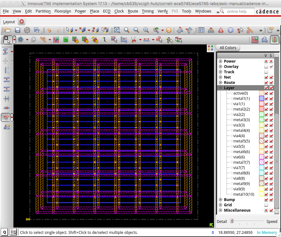
You can toggle the visibility of metal layers by using the panel on the right. Click the checkbox in the V column to toggle the visibility of the corresponding layer. You can also simply use the number keys on your keyboard. Pressing the 6 key will toggle M6 and pressing the 7 key will toggle M7. Zoom in on a via and toggle the visibility of the metal layers to see how Cadence Innovus has automatically inserted a via stack that goes from M1 all the way up to M6 or M7.
Now that we have finished our basic power planning we can do the initial
placement and routing of the standard cells using the place_design
command:
innovus> place_design
The following screen capture illustrates what you should see: the gates have been placed underneath a sea of wiring on the various metal layers.
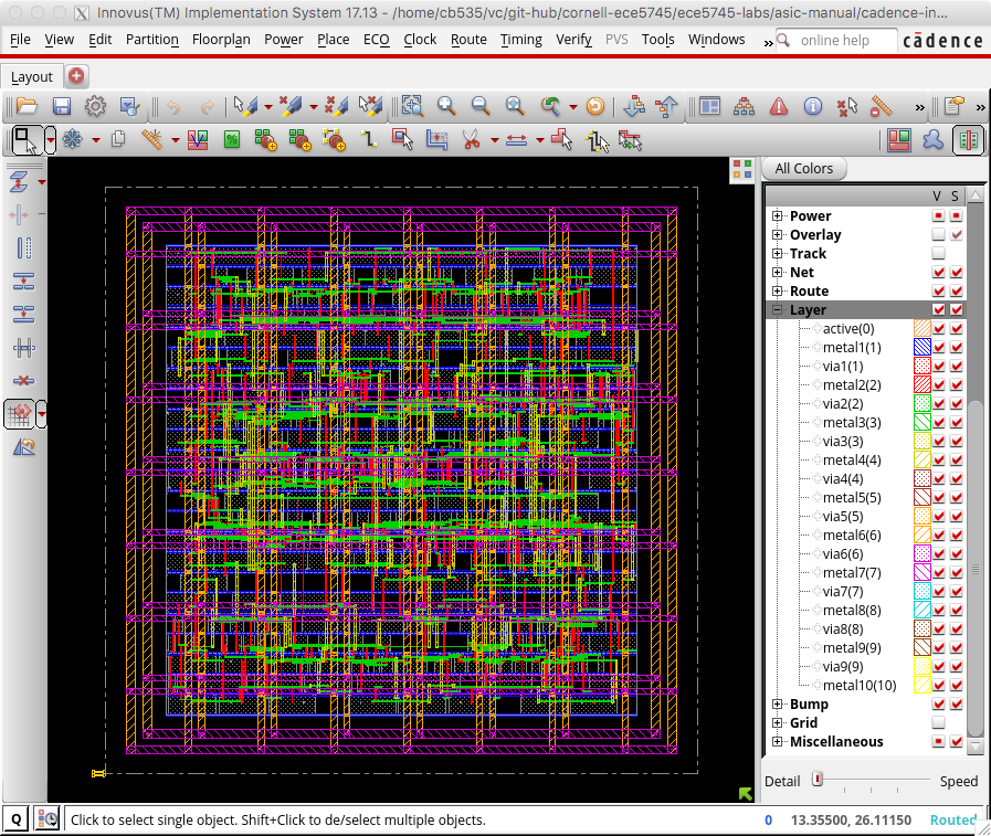
Note that Cadence Innovus has only done a very preliminary routing, primarily to help improve placement. You can use the Amobea workspace to help visualize how modules are mapped across the chip. Choose Windows > Workspaces > Amoeba from the menu. However, we recommend using the design browser to help visualize how modules are mapped across the chip. Here are the steps:
- Choose Windows > Workspaces > Design Browser + Physical from the menu
- Hide all of the metal layers by pressing the number keys
- Browse the design hierarchy using the panel on the left
- Right click on a module, click Highlight, select a color
In this way you can view where various modules are located on the chip.
The following screen capture illustrates the location of the five
MinMaxUnit modules.
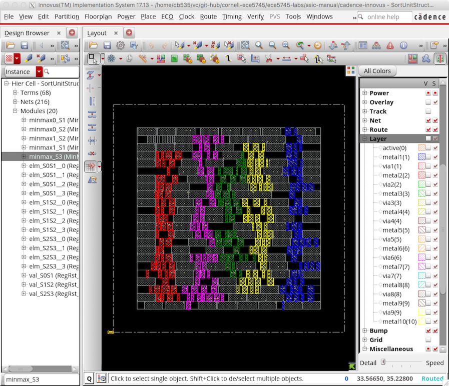
Notice how Cadence Innovus has grouped each module together. The placement algorithm tries to keep connected standard cells close together to minimize wiring.
The next step is to assign IO pin location for our block-level design. Since this is not a full chip with IOcells, or a hierarchical block, we don’t really care exactly where all of the pins line up, so we’ll let the tool assign the location for all of the pins.
innovus> assignIoPins -pin *
The next step is to improve the quality of the clock tree routing. First,
let’s display just the clock tree so we can clearly see the impact of
optimized clock tree routing. In the right panel click on Net and then
deselect the checkbox in the V column next to Signal, Special Net,
Power, and Ground so that only Clock is selected. You should be
able to see the clock snaking around the chip connecting the clock port
of all of the registers. Now use the ccopt_design command to optimize
the clock tree routing.
innovus> ccopt_design
If you watch closely you should see a significant difference in the clock tree routing before and after optimization. The following screen capture illustrates the optimized clock tree routing.
The routes are straighter, shorter, and well balanced. This will result in much lower clock skew.
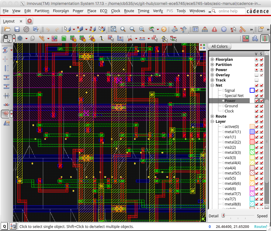
To avoid hold time violations (situations where the contamination delay is smaller than the hold time and new data arrives too quickly) we include the following commands:
 innovus> setOptMode -holdFixingCells {BUF_X1}
 innovus> setOptMode -holdTargetSlack 0.013 -setupTargetSlack 0.044;
 innovus> optDesign -postCTS -outDir timingReports -prefix postCTS_hold -hold
Here, we specified a list of buffer cells to the tool from stdcells.v that
innovus can use to add in delays to paths that violate the hold time
constraint. We then tell innovus our hold and setup time constraints, in
nanoseconds, these numbers were derived from the .lib file. Then, we
actually fix any violating paths using the optDesign command.
If you look into the output of optDesign, you should see the following section:
*** Finished Core Fixing (fixHold) cpu=0:00:00.6 real=0:00:01.0 totSessionCpu=0:01:30 mem=1745.2M density=71.079% ***
*info:
*info: Added a total of 51 cells to fix/reduce hold violation
*info:
*info: Summary:
*info:      51 cells of type ‘BUF_X1’ used
This means that as a result of our hold time optimization, we have added 51 buffer cells to the netlist.
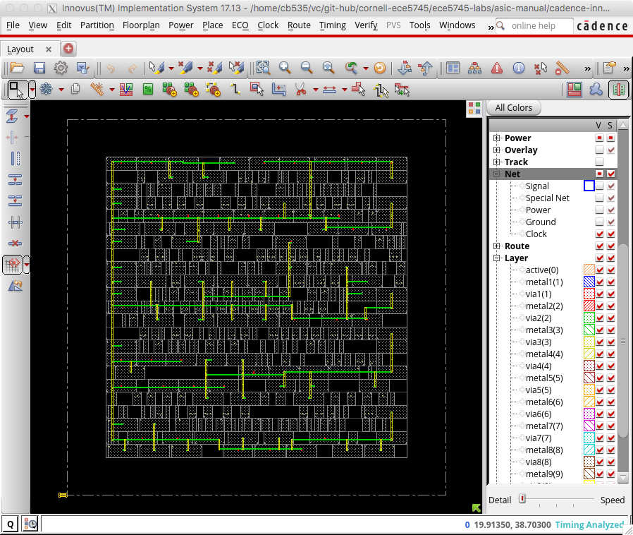
The next step is to improve the quality of the signal routing. Display
just the signals but not the power and ground routing by clicking on the
checkbox in the V column next to Signal in the left panel. Then use the
routeDesign command to optimize the signal routing. We follow this with
another iteration of optDesign to fix any violating paths that were
created during routeDesign.
 innovus> routeDesign
 innovus> optDesign -postRoute -outDir timingReports -prefix postRoute_hold -hold
If you watch closely you should see a significant difference in the signal routing before and after optimization. The following screen capture illustrates the optimized signal routing.
Again the routes are straighter and shorter. This will reduce the interconnect resistance and capacitance and thus improve the delay and energy of our design.
The final step is to insert “filler” cells. Filler cells are essentially empty standard cells whose sole purpose is to connect the wells across each standard cell row.
 innovus> setFillerMode -corePrefix FILL -core "FILLCELL_X4 FILLCELL_X2 FILLCELL_X1"
 innovus> addFiller
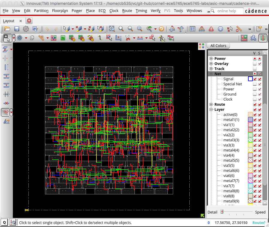
Zoom in to see some of the detailed routing and take a moment to appreciate how much effort the tools have done for us automatically to synthesize, place, and route this design. The following screen capture shows some of this detailed routing.
Notice how each metal layer always goes in the same direction. So M2 is always vertical, M3 is always horizontal, M4 is always vertical, etc. This helps reduce capacitive coupling across layers and also simplifies the routing algorithm. Actually, if you look closely in the above screen shot you can see situations on M2 (red) and M3 (green) where the router has generated a little “jog” meaning that on a single layer the wire goes both vertically and horizontally. This is an example of the sophisticated algorithms used in these tools.
Our design is now on silicon! Obviously there are many more steps required before you can really tape out a chip. We would need to add an I/O ring with pads so we can connect the chip to the package, we would need to do further verification, and additional optimization.
For example, one thing we want to do is verify that the gate-level
netlist matches what is really in the final layout. We can do this using
the verifyConnectivity command. We can also do a preliminary “design
rule check” to make sure that the generated metal interconnect does not
violate any design rules with the verify_drc command.
 innovus> verifyConnectivity
 innovus> verify_drc
Now we can generate various output files. We might want to save the final gate-level netlist for the chip, since Cadence Innovus will often insert new cells or change cells during its optimization passes.
innovus> saveNetlist post-par.v
We can also extract resistance and capacitance for the metal interconnect
and write this to a special .spef file. This file can be used for later
timing and/or power analysis.
 innovus> extractRC
 innovus> rcOut -rc_corner typical -spef post-par.spef
You may get an error regarding open nets. This is actually more of a warning message, and for the purposes of RC extraction we can ignore this.
We also need to extract delay information and write this to an
.sdf(Standard Delay Format) file, which we’ll use for our
back-annotated gate-level simulations.
innovus> write_sdf post-par.sdf -interconn all -setuphold split
Finally, we of course need to generate the real layout as a .gds file. This
is what we will send to the foundry when we are ready to tapeout the
chip.
 innovus> streamOut post-par.gds \
            -merge "$env(ECE5745_STDCELLS)/stdcells.gds" \
            -mapFile "$env(ECE5745_STDCELLS)/rtk-stream-out.map"
We can also use Cadence Innovus to do timing, area, and power analysis similar to what we did with Synopsys DC. These post-place-and-route results will be much more accurate than the preliminary post-synthesis results. Let’s start with a basic timing report.
 innovus> report_timing
 ...
 Other End Arrival Time          0.000
 - Setup                         0.045
 + Phase Shift                   0.600
 = Required Time                 0.555
 - Arrival Time                  0.502
 = Slack Time                    0.053
     Clock Rise Edge                 0.000
     + Clock Network Latency (Prop)  0.000
     = Beginpoint Arrival Time       0.000
     +-----------------------------------------------------------------------------------------------+
     |                Instance                |     Arc      |   Cell   | Delay | Arrival | Required |
     |                                        |              |          |       |  Time   |   Time   |
     |----------------------------------------+--------------+----------+-------+---------+----------|
     | elm_S1S2__2/out_reg[3]                 | CK ^         |          |       |   0.000 |    0.053 |
     | elm_S1S2__2/out_reg[3]                 | CK ^ -> Q ^  | DFF_X1   | 0.090 |   0.090 |    0.143 |
     | minmax0_S2/FE_DBTC3_elm_S1S2__2__out_3 | A ^ -> ZN v  | INV_X1   | 0.013 |   0.104 |    0.156 |
     | minmax0_S2/U14                         | A2 v -> ZN v | AND2_X1  | 0.029 |   0.133 |    0.186 |
     | minmax0_S2/U7                          | A2 v -> ZN v | OR2_X1   | 0.048 |   0.181 |    0.234 |
     | minmax0_S2/U10                         | A2 v -> ZN ^ | NOR2_X1  | 0.030 |   0.211 |    0.264 |
     | minmax0_S2/U35                         | A1 ^ -> ZN v | NOR2_X1  | 0.011 |   0.222 |    0.275 |
     | minmax0_S2/U11                         | A1 v -> ZN ^ | NOR2_X1  | 0.025 |   0.247 |    0.300 |
     | minmax0_S2/U38                         | A1 ^ -> ZN v | NOR3_X1  | 0.012 |   0.258 |    0.311 |
     | minmax0_S2/U65                         | A1 v -> ZN ^ | OAI22_X1 | 0.026 |   0.284 |    0.337 |
     | minmax0_S2/U13                         | A1 ^ -> ZN v | NAND2_X1 | 0.077 |   0.362 |    0.415 |
     | minmax0_S2/U33                         | A v -> ZN ^  | INV_X1   | 0.109 |   0.471 |    0.524 |
     | minmax0_S2/U60                         | A2 ^ -> ZN v | OAI22_X1 | 0.032 |   0.502 |    0.555 |
     | elm_S2S3__1/out_reg[7]                 | D v          | DFF_X1   | 0.000 |   0.502 |    0.555 |
     +-----------------------------------------------------------------------------------------------+
Note that for these results we used a target clock period of 0.6ns. This was the shortest clock period which still met timing without any negative slack during synthesis. From the above report we can see that our design is still meeting timing even after place-and-route. Note that it is very likely that the critical path identified by Synsopsys DC after synthesis will not be the same critical path identified by Cadence Innovus after place-and-route. This is because Synopsys DC can only guess the final placement of the cells and interconnect during static timing analysis, while Cadence Innovus can use the real placement of the cells and interconnect during static timing analysis. For the same reason, there is no guarantee that if your design meets timing after synthesis that it will still meet timing after place-and-route! It is very possible that your design will meet timing after synthesis and then will not meet timing after place-and-route. If your design does not meet timing after place-and-route you must go back and use a longer target clock period for synthesis!
You can use the following steps in Cadence Innovus to display where the critical path is on the actual chip.
- Choose Timing > Debug Timing from the menu
- Click OK in the pop-up window
- Right click on first path in the Path List
- Choose Highlight > Only This Path > Color
You can also use the Design Browser to highlight specific modules to
visualize how the critical path is routed across the chip between these
modules. The following screen capture illustrates the critical path in
our three-stage sort unit. From the above timing report we know the
critical path basically goes through the minmax0_S2 module, so we have
highlighted that module in red using the Design Browser. Cadence Innovus
has worked hard in both placement and routing to keep the critical path
short. If your critical path stretches across the entire chip you may
need to take extra steps such as explicit floorplanning or hierarchical
design to help the tools produce a better quality of result.
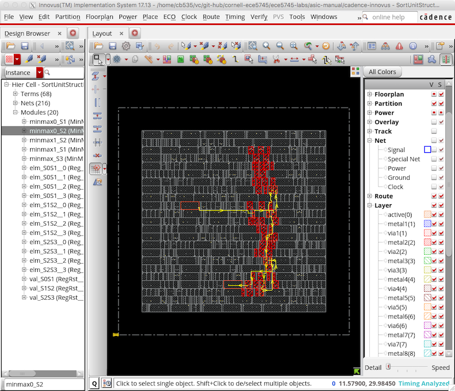
As in Synopsys DC, the report_area command can show the area each
module uses and can enable detailed area breakdown analysis. These area
results will be far more accurate than the post-synthesis results.
 innovus> report_area
  Depth  Name                          #Inst  Area (um^2)
  --------------------------------------------------------
  0      SortUnitStructRTL__nbits_8    369    709.688
  1      elm_S1S2__2                   8      36.176
  1      val_S1S2                      3      5.852
  1      minmax0_S1                    58     53.998
  1      elm_S0S1__3                   8      36.176
  1      minmax1_S2                    54     52.934
  1      elm_S0S1__0                   8      36.176
  1      elm_S2S3__0                   8      36.176
  1      elm_S2S3__1                   8      36.176
  1      minmax1_S1                    53     52.934
  1      elm_S1S2__1                   8      36.176
  1      val_S0S1                      3      5.852
  1      elm_S0S1__2                   8      36.176
  1      elm_S2S3__3                   8      36.176
  1      elm_S1S2__3                   8      36.176
  1      val_S2S3                      3      5.852
  1      minmax0_S2                    57     54.264
  1      elm_S1S2__0                   8      36.176
  1      minmax_S3                     42     43.89
  1      elm_S0S1__1                   8      36.176
  1      elm_S2S3__2                   8      36.176
The #Inst column indicates the number of non-filler cells in that
module. There are a total of 369 standard cells in the design. Each
register has eight standard cells; eight flip-flops since it is an
eight-bit register. The MinMaxUnits have a different number of cells
since they have been optimized differently. The MinMaxUnits consume
about ~40% of the area.
As in Synopsys DC, the report_power command can show how much power
each module consumes. Note that this power analysis is still not that
useful yet, since at this stage of the flow the power analysis is still
based purely on statistical activity factor estimation. We will do more
realistic power analysis in the next section.
innovus> report_power -hierarchy all
Finally, we go ahead and exit Cadence Innovus.
innovus> exit
We can now look at the actual .gds file for our design to see the final
layout including all of the cells and the interconnect using the
open-source Klayout GDS viewer. Choose Display > Full Hierarchy from
the menu to display the entire design. Zoom in and out to see the
individual transistors as well as the entire chip.
 % cd $TOPDIR/asic-manual/cadence-innovus
 % klayout -l $ECE5745_STDCELLS/klayout.lyp post-par.gds
The following screen capture illutrates using Klayout to view the layout for the entire sort unit.
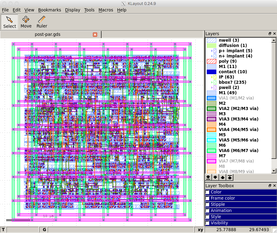
The following figure shows a zoomed portion of the layout. You can clearly see the active layer inside the standard cells along with the signal routing on the lower metal layers. The power routing on the upper metal layers has been hiddent for clarity.
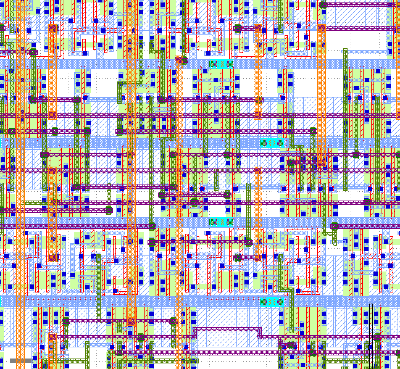
To Do On Your Own: Try increasing the bitwidth of the sort unit and see how this impacts the timing and/or area. For example, experiment with a sort unit capable of sorting 32-bit or 64-bit values. You will need to adjust the test harness and simulation driver appropriately.
Try flattening the design during synthesis by using this command:
dc_shell> compile -ungroup_all
or try using the compile_ultra command with (or without) flattening.
Then push the resulting design through place-and-route to see if this
improves the quality of results with respect to timing and/or area.
dc_shell> compile_ultra -no_autoungroup
You can put a sequence of commands in a .tcl file and then run Cadence
Innovus using those commands in one step like this:
 % cd $TOPDIR/asic-manual/cadence-innovus
 % innovus -64 -no_gui -files init.tcl
The -no_gui command prevents Cadence Innovus from opening the GUI which
can make interacting with the tool much faster. So consider placing the
commands from this section into a .tcl file to make it easy to rerun
Cadence Innovus.
Using Synopsys VCS for Back-Annotated Gate-Level Simulation
Before place and route, we used Synopsys VCS to do 4-state simulation,
and gate-level simulation. This time, we’ll be using VCS to perform a
back-annotated gate-level simulation. The key difference between the
previous gate-level simulation and this one is that in this case,
we’ll be using an .sdf file to annotate delays in the gate-level
simulation. In previous simulations, we only see signals change
on the clock edge; however, with a back-annotated simulation, we’ll
know more precisely when signals are arriving by using the delay
information provided by the .sdf. This means that running a
back-annotated simulation with a cycle time that is too fast will
cause the design to fail! Back-annotated simulations are also useful
for detecting hold-time violations.
Given the more realistic timing implications of a back-annotated
simulation, we need to be more careful about the cycle time, input
delay, and output delay that we provide to vcs. We’ll start by creating
a build directory for our post-synth run of vcs, and output directories
for the .vcd and .saif that we’ll generate for power analysis.
% mkdir -p $TOPDIR/asic-manual/vcs-postpnr-build
% cd $TOPDIR/asic-manual/vcs-postpnr-build
Then we’ll run vcs and ./simv to run our gate-level simulation on the sort-rtl-struct-random simulator testbench. Notice the differences between this command and the fast functional gate-level simulation command:
% vcs ../cadence-innovus/post-par.v $ECE5745_STDCELLS/stdcells.v -full64 -sverilog +incdir+../../sim/build +lint=all -xprop=tmerge -top SortUnitStructRTL__nbits_8_tb ../../sim/build/SortUnitStructRTL__nbits_8_sort-rtl-struct-random_tb.v +sdfverbose -sdf min:SortUnitStructRTL__nbits_8_tb.DUT:../cadence-innovus/post-par.sdf +define+CYCLE_TIME=0.6 +define+VTB_INPUT_DELAY=0.03 +define+VTB_OUTPUT_ASSERT_DELAY=0.57 +vcs+dumpvars+SortUnitStructRTL__nbits_8_sort-rtl-struct-random_vcs.vcd +neg_tchk -override_timescale=1ns/1ps
% ./simv
This time, we add the flag +neg_tchk, which enables negative values in
timing checks. Negative values in timing checks are important for cells
which have negative hold times, for example. We also include the
+sdfverbose flag which reads in the post-par.sdf. Note that we also
assign non-zero values for +define+VTB_INPUT_DELAY and
+define+VTB_OUTPUT_ASSERT_DELAY. These values are based on the input
and output delays we set during the Synopsys DC synthesis step which you
might recall was 0.05*clock_period. Note that we assert the value at
the clock constraint minus the output delay. This ensures that the signal
arrives and is stable by a margin of the output delay. Including these
macros will ensure that our timing checks will actually mean something.
Without this, our simulations may pass because data arrives before the
clock edge, even if it does not arrive before the output delay. In such a
case, the timing checks will be completely bogus. To illustrate how useful
these timing checks can be, lets run another simulation where we try to push
the design to run too quickly. Here, we reduce the cycle time down to 0.45 ns:
% cd $TOPDIR/asic-manual/vcs-postpnr-build
% vcs ../cadence-innovus/post-par.v $ECE5745_STDCELLS/stdcells.v -full64 -sverilog +incdir+../../sim/build +lint=all -xprop=tmerge -top SortUnitStructRTL__nbits_8_tb ../../sim/build/SortUnitStructRTL__nbits_8_sort-rtl-struct-random_tb.v +sdfverbose -sdf max:SortUnitStructRTL__nbits_8_tb.DUT:../cadence-innovus/post-par.sdf +define+CYCLE_TIME=0.45 +define+VTB_INPUT_DELAY=0.03 +define+VTB_OUTPUT_ASSERT_DELAY=0.42 +vcs+dumpvars+SortUnitStructRTL__nbits_8_sort-rtl-struct-random_vcs.vcd +neg_tchk -override_timescale=1ns/1ps
% ./simv
Note that we also annotated the sdf using the maximum delays, due to the
-sdf max:... flag. It is important to do a check using the maximum delays
for setup time checks, and using minimum delays for hold time checks.
Here, we can see the violating flip-flop, and the subsequent testbench
failure. Note that you resulting netlist and layout may be slightly different
than the one referenced here, so if your timing violation looks slightly
different, or you do not yet have a timing violation, that is ok! Feel free
to run your simulation even faster if that is the case, by changing the
CYCLE_TIME and VTB_OUTPUT_ASSERT_DELAY macros.
"/work/global/brg/install/adk-pkgs/freepdk-45nm/stdview/stdcells.v", 2123: Timing violation in SortUnitStructRTL__nbits_8_tb.DUT.elm_S1S2__0.\out_reg[1]
    $setuphold( posedge CK:10129, negedge D:10110, limits: (44,10) );


The test bench received a value containing X/Z's! Please note
that the VTB is pessmistic about X's and you should make sure
all output ports of your DUT does not produce X's after reset.
- Timestamp      : 11 (default unit: ns)
- Cycle number   : 23 (variable: cycle_count)
- line number    : line 22 in SortUnitStructRTL__nbits_8_sort-rtl-struct-random_tb.v.cases
- port name      : out[2] (out[2] in Verilog)
- expected value : 0xf5
- actual value   : 0xfX
Let’s re-run the simulation at the correct clock speed to obtain the right vcd for saif generation.
% vcs ../cadence-innovus/post-par.v $ECE5745_STDCELLS/stdcells.v -full64 -sverilog +incdir+../../sim/build +lint=all -xprop=tmerge -top SortUnitStructRTL__nbits_8_tb ../../sim/build/SortUnitStructRTL__nbits_8_sort-rtl-struct-random_tb.v +sdfverbose -sdf min:SortUnitStructRTL__nbits_8_tb.DUT:../cadence-innovus/post-par.sdf +define+CYCLE_TIME=0.6 +define+VTB_INPUT_DELAY=0.03 +define+VTB_OUTPUT_ASSERT_DELAY=0.57 +vcs+dumpvars+SortUnitStructRTL__nbits_8_sort-rtl-struct-random_vcs.vcd +neg_tchk -override_timescale=1ns/1ps
% ./simv
The .vcd file contains information about the state of every net in the
design on every cycle. This can make these .vcd files very large and
thus slow to analyze. For average power analysis, we only need to know
the activity factor on each net. We can use the vcd2saif tool to
convert .vcd files into .saif files. An .saif file only contains a
single average activity factor for every net.
% cd $TOPDIR/asic-manual/vcs-postpnr-build
% vcd2saif -input ./SortUnitStructRTL__nbits_8_sort-rtl-struct-random_vcs.vcd -output ./SortUnitStructRTL__nbits_8_sort-rtl-struct-random.saif
Take a look at the vcd file from this simulation. Here we can see some subcycle delays that shows us how long it takes for data to stabilize before the following cycle, super cool! This is showing the first stage of the sort unit pipeline. It shows the input and output of the stage 0 pipeline registers, the input/output of the two stage 0 minmax units, and the input and output of the stage 1 pipeline registers.
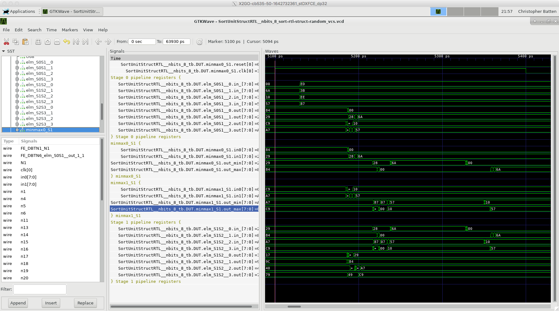
Using Synopsys PrimeTime for Power Analysis
Synopsys PrimeTime (PT) is primarily used for very accurate “sign-off” static timing analysis (more accurate than the analysis performed by Synopsys DC and Cadence Innovus), but in this course, we will only use Synopsys PT for power analysis. There are many ways to perform power analysis. As mentioned earlier, the post-synthesis and post-place-and-route power reports use statistical power analysis where we simply assume some toggle probability on each net. For more accurate power analysis we need to find out the actual activity for every net for a given experiment. One way to do this is to perform post-place-and-route gate-level simulation.
We start by creating a subdirectory for our work, and then launching Synopsys PT.
 % mkdir -p $TOPDIR/asic-manual/synopsys-pt
 % cd $TOPDIR/asic-manual/synopsys-pt
 % pt_shell
To make it easier to copy-and-paste commands from this document, we tell
Synopsys PT to ignore the prefix pt_shell> using the following:
pt_shell> alias "pt_shell>" ""
We begin by setting the target_library and link_library variables as
before.
 pt_shell> set_app_var target_library "$env(ECE5745_STDCELLS)/stdcells.db"
 pt_shell> set_app_var link_library   "* $env(ECE5745_STDCELLS)/stdcells.db"
Since Synopsys PT is primarily used for static timing analysis, we need to explicitly tell Synopsys PT that we want to use it for power analysis.
pt_shell> set_app_var power_enable_analysis true
We now read in the gate-level netlist, tell Synopsys PT we want to do power analysis for the top-level module, and link the design (i.e., recursively resolve all of the module references starting from the top-level module).
 pt_shell> read_verilog   "../cadence-innovus/post-par.v"
 pt_shell> current_design SortUnitStructRTL__nbits_8
 pt_shell> link_design
In order to do power analysis, Synopsys PT needs to know the clock period. Here we will set the clock frequency to be the same as the initial clock constraint, but note that this is only valid if our design actually met timing. If our design has negative slack, then this means we cannot actually run the design at the target clock frequency and we will need to iterate to meet timing.
pt_shell> create_clock clk -name ideal_clock1 -period 0.6
We are now ready to read in the actual activity factors which will be
used for power analysis. The .saif file comes from a .vcd file which
in turn came from running a simulation with a test harness. We need to
strip off part of the instance names in the .saif file since the
gate-level netlist does not have this test harness.
pt_shell> read_saif "../../asic-manual/vcs-postpnr-build/SortUnitStructRTL__nbits_8_sort-rtl-struct-random.saif" -strip_path "SortUnitStructRTL__nbits_8_tb/DUT"
The .db file includes parasitic capacitance estimates for every pin of
every standard cell, but to improve the accuracy of power analysis, we
also need to include parasitic capacitances from the interconnect. Recall
that we used Cadence Innovus to generate exactly this information in a
.spef file. So we now read in these additional parasitic capacitance
values for every net in the gate-level netlist.
pt_shell> read_parasitics -format spef "../cadence-innovus/post-par.spef"
We now have everything we need to perform the power analysis: (1) the
activity factor of a subset set of the nets, (2) the capacitance of every
net/port, (3) the supply voltage, and (4) the clock frequency. We use the
update_power command to propagate activity factors to unannotated nest
and to estimate the power of our design.
pt_shell> update_power
We can use the report_power command to show a high-level overview of
how much power the sort unit consumes.
 pt_shell> report_power -nosplit
 ...
                Internal Switching Leakage Total
 Power Group    Power    Power     Power   Power   (     %)
 ----------------------------------------------------------
 clock_network  3.8e-04  0.0       0.0     3.8e-04 (25.76%)
 register       4.1e-04  8.2e-05   7.8e-06 5.0e-04 (34.06%)
 combinational  2.4e-04  3.4e-04   6.6e-06 5.9e-04 (40.18%)
 sequential     0.0      0.0       0.0     0.0     ( 0.00%)
 memory         0.0      0.0       0.0     0.0     ( 0.00%)
 io_pad         0.0      0.0       0.0     0.0     ( 0.00%)
 black_box      0.0      0.0       0.0     0.0     ( 0.00%)

  Net Switching Power  = 4.267e-04   (28.82%)
  Cell Internal Power  = 1.039e-03   (70.20%)
  Cell Leakage Power   = 1.450e-05   ( 0.98%)
                         ---------
  Total Power          = 1.481e-03  (100.00%)
These numbers are in Watts. We can see that the sort unit consumes ~1.5mW of power when processing random input data. Power is the rate change of energy (i.e., energy divided by execution time), so the total energy is just the product of the total power, the number of cycles, and the cycle time. When we ran the sort unit simulator at the beginning of the tutorial, we saw that the simulation required 105 cycles. Assuming our sort unit runs as 0.6ns, this means the total energy is 1.5mW * 105 * 0.6ns = 95pJ. Since we are doing 100 sorts, this corresponds to about 1pJ per sort.
The power is broken down into internal, switching, and leakage power. Internal and switching power are both forms of dynamic power, while leakage power is a form of static power. Notice that in this case, the dynamic power is much more significant than the static power. Internal power was described earlier in this tutorial, so you may want to revisit that section. Note that internal power includes short circuit power, but it can also include the local clock power internal to the cell. In this overview, the power is also broken down by the power consumed in the global clock network, registers, and combinational logic. Switching power is the power dissipated by the charging and discharging of the load capacitance at the output of each cell. Leakage power is the constant power due to subthreshold leakage. Sometimes we might want to factor out the static leakage power and focus more on the dynamic energy since including leakage power would mix energy and performance (i.e., using more cycles requires more leakage power even if we are not doing any more work during those cycles).
Although the above breakdown is somewhat useful, it is even more useful
to use the report_power command to show how much power each module
consumes in the design.
 pt_shell> report_power -nosplit -hierarchy
 ...
                             Int      Switch   Leak     Total
 Hierarchy                   Power    Power    Power    Power        %
 ---------------------------------------------------------------------
 SortUnitStructRTL__nbits_8  1.04e-03 4.27e-04 1.45e-05 1.48e-03 100.0
  elm_S2S3__0 (Reg_4)        6.17e-05 5.74e-07 6.30e-07 6.29e-05   4.3
  elm_S1S2__0 (Reg_8)        6.34e-05 6.60e-06 6.33e-07 7.06e-05   4.8
  elm_S2S3__1 (Reg_3)        6.50e-05 7.91e-06 6.33e-07 7.36e-05   5.0
  val_S0S1    (RegRst_0)     6.66e-06 6.89e-08 1.17e-07 6.85e-06   0.5
  elm_S1S2__1 (Reg_7)        6.56e-05 8.73e-06 6.32e-07 7.50e-05   5.1
  elm_S0S1__0 (Reg_0)        6.49e-05 6.99e-06 6.33e-07 7.26e-05   4.9
  elm_S2S3__2 (Reg_2)        6.46e-05 9.64e-06 6.33e-07 7.49e-05   5.1
  elm_S0S1__1 (Reg_11)       6.52e-05 8.31e-06 6.33e-07 7.42e-05   5.0
  minmax0_S1  (MinMaxUnit_0) 5.18e-05 7.10e-05 1.36e-06 1.24e-04   8.4
  elm_S2S3__3 (Reg_1)        6.42e-05 6.38e-07 6.32e-07 6.55e-05   4.4
  elm_S1S2__2 (Reg_6)        6.41e-05 9.20e-06 6.33e-07 7.39e-05   5.0
  elm_S0S1__2 (Reg_10)       6.57e-05 7.03e-06 6.33e-07 7.34e-05   5.0
  minmax0_S2  (MinMaxUnit_4) 4.93e-05 6.81e-05 1.39e-06 1.19e-04   8.0
  elm_S1S2__3 (Reg_5)        6.44e-05 8.12e-06 6.32e-07 7.31e-05   4.9
  elm_S0S1__3 (Reg_9)        6.61e-05 9.15e-06 6.33e-07 7.59e-05   5.1
  minmax1_S1  (MinMaxUnit_3) 5.20e-05 7.23e-05 1.36e-06 1.26e-04   8.5
  minmax1_S2  (MinMaxUnit_2) 4.91e-05 7.01e-05 1.33e-06 1.20e-04   8.1
  minmax_S3   (MinMaxUnit_1) 4.23e-05 6.21e-05 1.13e-06 1.06e-04   7.1
  val_S2S3    (RegRst_1)     6.65e-06 5.00e-08 1.17e-07 6.82e-06   0.5
  val_S1S2    (RegRst_2)     6.67e-06 6.84e-08 1.17e-07 6.85e-06   0.5
From this breakdown, you can see that each MinMaxUnit consumes about
twice as much power as each register.
Finally, we go ahead and exit Synopsys PT.
pt_shell> exit
To Do On Your Own: You can experiment with the power consumed when
executing a different dataset by simply reruning the simulation to
generate a new .vcd file, converting that file to an .saif file, and
then following the above steps again. Use the following commands to
generate an .saif file for a simulation where all of the input values
to the sort unit are zeros.
 % cd $TOPDIR/sim/build
 % ../tut3_pymtl/sort/sort-sim --impl rtl-struct --input zeros --stats --translate --dump-vtb
 num_cycles          = 105
 num_cycles_per_sort = 1.05
% cd $TOPDIR/asic-manual/vcs-rtl-build
% vcs ../../sim/build/SortUnitStructRTL__nbits_8__pickled.v -full64 -sverilog +incdir+../../sim/build +lint=all -xprop=tmerge -top SortUnitStructRTL__nbits_8_tb ../../sim/build/SortUnitStructRTL__nbits_8_sort-rtl-struct-zeros_tb.v +vcs+dumpvars+SortUnitStructRTL__nbits_8_sort-rtl-struct-zeros_vcs.vcd -override_timescale=1ns/1ns
% ./simv
% cd $TOPDIR/asic-manual/vcs-rtl-build
% vcd2saif -input ./vcd/SortUnitStructRTL__nbits_8_sort-rtl-struct-zeros_vcs.vcd -output ./saif/SortUnitStructRTL__nbits_8_sort-rtl-struct-zeros.saif
Do you think a stream of random data will consume more or less power
compared to a stream of zeros? Rerun Synopsys PT to find out. This means
you will need to read in the new .saif file. In other words, use the
following command:
pt_shell> read_saif "../../asic-manual/vcs-postpnr-build/SortUnitStructRTL__nbits_8_sort-rtl-struct-zeros.saif" -strip_path "SortUnitStructRTL__nbits_8_tb/DUT"
As with Synopsys DC, you can put a sequence of commands in a .tcl file
and then run Synopsys PT using those commands in one step like this:
 % cd $TOPDIR/asic-manual/synopsys-pt
 % pt_shell -file init.tcl
So consider placing the commands from this section into a .tcl file to
make it easy to rerun Synopsys PT.
Using Verilog RTL Models
Students are welcome to use Verilog instead of PyMTL3 to design their RTL models. Having said this, we will still exclusively use PyMTL3 for all test harnesses, FL/CL models, and simulation drivers. This really simplifies managing the course, and PyMTL3 is actually a very productive way to test/evaluate your Verilog RTL designs. We use PyMTL3’s Verilog import feature described in the Verilog tutorial to make all of this work. The following commands will run all of the tests on the Verilog implementation of the sort unit.
 % cd $TOPDIR/sim/build
 % rm -rf *
 % pytest ../tut4_verilog/sort --dump-vtb --test-verilog;
As before, the tests for the SortUnitStructRTL will fail. You can just
copy over your implementation of the MinMaxUnit from when you completed
the Verilog tutorial. If you have not completed the Verilog tutorial then
you might want to go back and do that now. Basically the MinMaxUnit
should look like this:
`ifndef TUT4_VERILOG_SORT_MIN_MAX_UNIT_V
`define TUT4_VERILOG_SORT_MIN_MAX_UNIT_V

module tut4_verilog_sort_MinMaxUnit
#(
  parameter p_nbits = 1
)(
  input  logic [p_nbits-1:0] in0,
  input  logic [p_nbits-1:0] in1,
  output logic [p_nbits-1:0] out_min,
  output logic [p_nbits-1:0] out_max
);

  always_comb begin

    // Find min/max

    if ( in0 >= in1 ) begin
      out_max = in0;
      out_min = in1;
    end
    else if ( in0 < in1 ) begin
      out_max = in1;
      out_min = in0;
    end

    // Handle case where there is an X in the input

    else begin
      out_min = 'x;
      out_max = 'x;
    end

  end

endmodule

`endif /* TUT4_VERILOG_SORT_MIN_MAX_UNIT_V */
After running the tests we use the sort unit simulator to translate the Verilog RTL model into Verilog and to dump the VCD file that we want to use for power analysis.
 % cd $TOPDIR/sim/build
 % ../tut4_verilog/sort/sort-sim --impl rtl-struct --stats --translate --dump-vtb
Take a moment to open up the translated Verilog which should be in a file
named SortUnitFlatRTL__nbits_8__pickled.v. You might ask, “Why do we
need to use PyMTL3 to translate the Verilog if we already have the
Verilog?” PyMTL3 will take care of preprocessing all of your Verilog RTL
code to ensure it is in a single Verilog file. This greatly simplifies
getting your design into the ASIC flow. This also ensures a one-to-one
match between the Verilog that was used to generate the VCD file and the
Verilog that is used in the ASIC flow.
Once you have tested your design and generated the single Verilog file and the VCD file, you can push the design through the ASIC flow using the exact same steps we used above. The PyMTL RTL and Verilog RTL designs should show similar results, but obviously they won’t be exactly the same since the source code is different.
To Do On Your Own
Use what you have learned so far to push the GCD Unit through the flow.
You can use either the PyMTL3 or Verilog GCD Unit provided along with
this tutorial. You will need to verify the GCD Unit works, generate the
corresponding Verilog RTL and VTB file using the GCD Unit simulator, run
a 4 state simulation and generate the corresponding .saif file, use
Synopsys DC to synthesize the design to a gate-level netlist, use Cadence
Innovus to place-and-route the design, and use Synopsys PT for power analysis.
Note that the GCD Unit will not pass 4-state simulation out of the box.
Think about how you can modify the RTL to avoid x’s from showing up on the
output. This will be important to think about as you make your own
designs in the labs.