ECE 5745 Tutorial 6: Automated ASIC Block Flow
- Author: Christopher Batten, Yanghui Ou, Jack Brzozowski
- Date: January 6, 2022
Table of Contents
- Introduction
- PyMTL-Based Testing, Simulation, Translation
- Getting Started Using Mflowgen
- Gathering RTL and Testbenches
- Using Synopsys VCS for 4-State RTL Simulation
- Using Synopsys Design Compiler for Synthesis
- Using Synopsys VCS for Fast Functional Gate-Level Simulation
- Using Synopsys PrimeTime for Post-Synth Power Analysis
- Using Cadence Innovus for Place-and-Route
- Using Synopsys VCS for Back-Annotated Gate-Level Simulation
- Performing Hold Fixing on a Design
- Using Synopsys PrimeTime for Post-Place-and-Route Power Analysis
- Reviewing the Flow Summary
- Using the Automated ASIC Flow for Design-Space Exploration
- Using Verilog RTL Models
- Pushing GCD Unit Through the Automated ASIC Flow
Introduction
The previous tutorial introduced students to the key tools used for
synthesis, place-and-route, and power analysis, but the previous tutorial
required students to enter commands manually for each tool. This is
obviously very tedious and error prone. An agile hardware design flow
demands automation to simplify rapidly exploring the area, energy, timing
design space of one or more designs. Luckily, Synopsys and Cadence tools
can be easily scripted using TCL, and even better, the ECE 5745 staff have
created steps for automating the entire flow using mflowgen.
The tutorial will describe how to take your designs from RTL to layout. Mflowgen makes it relatively easy to achieve this by using modular steps to piece together a set of scripts that generates all the files we’ll need to describe the final layout, and well as reports on power, timing, area, and much more. We often call such a set of scripts an “ASIC flow”. However, it is critical for students to avoid thinking of the ASIC flow as a black box. As in all engineering, garbage-in means garbage-out. If you are not careful it is all too easy to use the ASIC flow to analyze a completely invalid design. This tutorial assumes you have already completed the tutorials on Linux, Git, PyMTL, Verilog, and the Synopsys/Cadence ASIC tools.
The following diagram illustrates the five primary tools we will be using in ECE 5745. This is nearly the same flow diagram from the previous tutorial since in part 1 of this tutorial, we are essentially just automating the exact same steps.
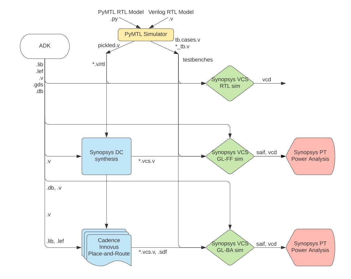
-
We use the PyMTL framework to test, verify, and evaluate the execution time (in cycles) of our design. This part of the flow is exactly the same as ECE 4750. Note that we can write our RTL models in either PyMTL or Verilog. Once we are sure our design is working correctly, we can then start to push the design through the flow. The ASIC flow requires Verilog RTL as an input, so we can use PyMTL’s automatic translation tool to translate PyMTL RTL models into Verilog RTL.
-
We use Synopsys VCS to compile and run both 4-state RTL and gate-level simulations. These simulations help us to build confidence in our design as we push our designs through different stages of the flow. From these simulations, we also generate waveforms in
.vcd(Verilog Change Dump) format, and we usevcd2saifto convert these waveforms into per-net average activity factors stored in.saifformat. These activity factors will be used for power analysis. Gate-level simulation is an extremely valuable tool for ensuring the tools did not optimize something away which impacts the correctness of the design, and also provides an avenue for obtaining a more accurate power analysis than RTL simulation. Though Static Timing Analysis (STA) is much better because it analyzes all paths, GL simulation also serves as a backup to check for hold and setup time violations (chip designers must be paranoid!) -
We use Synopsys Design Compiler (DC) to synthesize our design, which means to transform the Verilog RTL model into a Verilog gate-level netlist where all of the gates are selected from a standard cell library. We need to provide Synopsys DC with higher-level characterization information about our standard cell library.
-
We use Cadence Innovus to place-and-route our design, which means to place all of the gates in the gate-level netlist into rows on the chip and then to generate the metal wires that connect all of the gates together. Cadence Innovus will also handle power and clock routing. We need to provide Cadence Innovus with lower-level characterization information about our standard cell library. Cadence Innovus also generates reports that can be used to more accurately characterize area and timing.
-
We use Synopsys PrimeTime (PT) to perform power-analysis of our design. This requires switching activity information for every net in the design (which comes from the PyMTL simulator) and parasitic capacitance information for every net in the design (which comes from Cadence Innovus). Synopsys PT puts the switching activity, capacitance, clock frequency, and voltage together to estimate the power consumption of every net and thus every module in the design.
Extensive documentation is provided by Synopsys and Cadence for Design Compiler, Cadence Innovus, and Synopsys PrimeTime. We have organized this documentation and made it available to you on the public course webpage. The username/password was distributed during lecture.
The first step is to source the setup script, clone this repository from GitHub, and define an environment variable to keep track of the top directory for the project.
 % source setup-ece5745.sh
 % mkdir -p $HOME/ece5745
 % cd $HOME/ece5745
 % git clone git@github.com:cornell-ece5745/ece5745-tut6-asic-flow
 % cd ece5745-tut6-asic-flow
 % TOPDIR=$PWD
PyMTL-Based Testing, Simulation, Translation
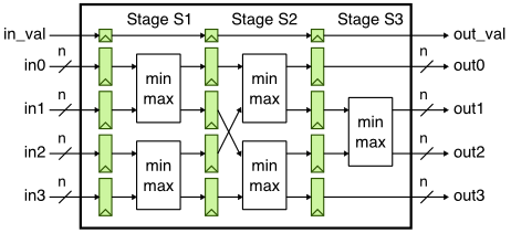
As in the previous tutorial, our goal is to characterize the area, energy, and timing for the sort unit from the PyMTL tutorial using the ASIC tools. As a reminder, the sort unit takes as input four integers and a valid bit and outputs those same four integers in increasing order with the valid bit. The sort unit is implemented using a three-stage pipelined, bitonic sorting network and the datapath is shown below.
Let’s start by running the tests for the sort unit and note that the
tests for the SortUnitStructRTL will fail. You can just copy over your
implementation of the MinMaxUnit from when you completed the PyMTL
tutorial. If you have not completed the PyMTL tutorial then go back and
do that now.
Basically the MinMaxUnit should look like this:
from pymtl3 import *

class MinMaxUnit( Component ):

  # Constructor

  def construct( s, nbits ):

    s.in0     = InPort ( nbits )
    s.in1     = InPort ( nbits )
    s.out_min = OutPort( nbits )
    s.out_max = OutPort( nbits )

    @update
    def block():

      if s.in0 >= s.in1:
        s.out_max @= s.in0
        s.out_min @= s.in1
      else:
        s.out_max @= s.in1
        s.out_min @= s.in0

  # Line tracing

  def line_trace( s ):
    return f"{s.in0}|{s.in1}(){s.out_min}|{s.out_max}"
Now running the following tests will pass.
 % mkdir -p $TOPDIR/sim/build
 % cd $TOPDIR/sim/build
 % pytest ../tut3_pymtl/sort
 % pytest ../tut3_pymtl/sort --test-verilog --dump-vtb
As we learned in the previous tutorial, the --test-verilog command line
option tells the PyMTL framework to first translate the sort unit into
Verilog, and then important it back into PyMTL to verify that the
translated Verilog is itself correct.
Let’s experiment with an example which is valid PyMTL code, but is
not translatable to illustrate the importance of testing with
--test-verilog. Instead of using an if statement to implement the
MinMaxUnit, maybe we want to be clever and use the built-in min and
max Python functions like this:
from pymtl3 import *

class MinMaxUnit( Component ):

  # Constructor

  def construct( s, nbits ):

    s.in0     = InPort ( nbits )
    s.in1     = InPort ( nbits )
    s.out_min = OutPort( nbits )
    s.out_max = OutPort( nbits )

    @update
    def block():
      s.out_max @= max( s.in0, s.in1 )
      s.out_min @= min( s.in0, s.in1 )
Rerun the tests on the pure-PyMTL implementation:
 % cd $TOPDIR/sim/build
 % pytest ../tut3_pymtl/sort/test/MinMaxUnit_test.py
All of the tests should pass, but now try running the tests with
--test-verilog.
 % cd $TOPDIR/sim/build
 % pytest ../tut3_pymtl/sort/test/MinMaxUnit_test.py --test-verilog
 % pytest ../tut3_pymtl/sort/test/MinMaxUnit_test.py -x --tb=short --test-verilog
...
E   pymtl3.passes.rtlir.errors.PyMTLSyntaxError:
E   In file /home/yo96/ece5745/ece5745-labs/sim/tut3_pymtl/sort/MinMaxUnit.py, Line 28, Col 18:
E     s.out_max @= max( s.in0, s.in1 )
E                 ^
E   - <_ast.Name object at 0x7f9d58048b50> function is not found!
The error message indicates that there is a translation error. In other
words, using the min/max functions is perfectly valid PyMTL code, but
the translation tool does not know how to translate these constructs into
Verilog. If you stick to the PyMTL usage rules posted on the course
website, your code will probably be translatable. However, it is not
that difficult to write reasonable PyMTL code that is not translatable,
and there is no guarantee the translation tool will catch translation
errors and produce such a nice error message as shown above. Translation
errors can result in run-time errors when you use --test-verilog or
they can even simulate correctly but produce errors when you try and
synthesize the design. So remember to always use --test-verilog before
using the ASIC flow, and to look for errors from the translation tool,
Verilator, and/or Synopsys DC. Make sure to fix the MinMaxUnit and re-run
the tests using the --dump-vtb flag before moving on!
After running the tests we use the sort unit simulator to do the final
translation into Verilog and to dump the vtb (Verilog TestBench) file
that will allow us to do 4-state RTL simulation using Synopsys VCS.
 % cd $TOPDIR/sim/build
 % ../tut3_pymtl/sort/sort-sim --impl rtl-struct --stats --translate --dump-vtb
 num_cycles          = 105
 num_cycles_per_sort = 1.05
We now have both the translated Verilog for the sort unit, and the Verilog
Testbench and Verilog testbench cases files for all of our tests and simulations,
so we are ready to use the ASIC flow to quantitatively evaluate the area,
energy, and timing of our design. It is extremely important to use the
--dump-vtb flag on both the tests that you want to use for VCS simulation, and
the simulation inputs that you want to use for power analysis. The Verilog
Testbench is a translated version of your PyMTL simulation that VCS will use to
run its simulation. Without these testbenches, these simulations will not be run
by the automated flow. Make sure that you have these files dumped in your build
folder before moving onto the ASIC flow. For the purposes of showing off some
features of the ASIC flow, lets run a few more simulations before moving on:
 % cd $TOPDIR/sim/build
 % ../tut3_pymtl/sort/sort-sim --impl rtl-struct --input sorted-fwd --stats --translate --dump-vtb
 % ../tut3_pymtl/sort/sort-sim --impl rtl-struct --input sorted-rev --stats --translate --dump-vtb
 % ../tut3_pymtl/sort/sort-sim --impl rtl-struct --input zeros --stats --translate --dump-vtb
Getting Started Using Mflowgen
Mflowgen is a modular flow specification and build-system generator for ASIC and FPGA design-space exploration and Electronic Design Automation (EDA) being developed at Stanford University. The ECE5745 staff have been working with the folks at Stanford to help build this flow, and we are extremely excited to be bringing mflowgen into the ECE5745 course this year. Let’s take a look into how we can start setting up and configuring an mflowgen build:
 % cd $TOPDIR/sim/tut3_pymtl/sort
 % cat .mflowgen.yml

 construct: ../../../asic/SortUnitStructRTL_BlockFlow.py
The construct key in your .mflowgen.yml file tells mflowgen which flow.py
configuration script to use for this design folder. The .mflowgen.yml file must
exist in the folder of the design you are trying to build a flow for. We can
create a build using the mflowgen run command. The --design argument is
simply the path to the .mflowgen.yml file. We’ll create an asic build for the
sort unit according to the configuration in SortUnitStructRTL_BlockFlow.py.
 % mkdir -p $TOPDIR/asic/build
 % cd $TOPDIR/asic/build
 % mflowgen run --design ../../sim/tut3_pymtl/sort
Targets: run "make list" and "make status"
Run the targets make list and make status to get a sense for what’s included in the flow the ECE5745 staff have created for you.
 % make list
Generic Targets:

 - list      -- List all steps
 - status    -- Print build status for each step
 - runtimes  -- Print runtimes for each step
 - graph     -- Generate a PDF of the step dependency graph
 - clean-all -- Remove all build directories
 - clean-N   -- Clean target N
 - info-N    -- Print configured info for step N
 - diff-N    -- Diff target N

Targets:

 -   0 : build-info
 -   1 : ece5745-block-gather
 -   2 : freepdk-45nm
 -   3 : brg-RTL-4-state-vcssim
 -   4 : brg-synopsys-dc-synthesis
 -   5 : PostSynth-Gate-Level-Simulation
 -   6 : brg-cadence-innovus-init
 -   7 : PostSynth-power-analysis
 -   8 : brg-cadence-innovus-blocksetup
 -   9 : brg-cadence-innovus-pnr
 -  10 : brg-cadence-innovus-signoff
 -  11 : PostPNR-Gate-Level-Simulation
 -  12 : PostPNR-power-analysis
 -  13 : brg-flow-summary

 % make status

Upcoming build order:

 - 0-build-info
 - 1-ece5745-block-gather
 - 2-freepdk-45nm
 - 3-brg-RTL-4-state-vcssim
 - 4-brg-synopsys-dc-synthesis
 - 5-PostSynth-Gate-Level-Simulation
 - 6-brg-cadence-innovus-init
 - 7-PostSynth-power-analysis
 - 8-brg-cadence-innovus-blocksetup
 - 9-brg-cadence-innovus-pnr
 - 10-brg-cadence-innovus-signoff
 - 11-PostPNR-Gate-Level-Simulation
 - 12-PostPNR-power-analysis
 - 13-brg-flow-summary

Status:

 - build -> 0   : build-info
 - build -> 1   : ece5745-block-gather
 - build -> 2   : freepdk-45nm
 - build -> 3   : brg-RTL-4-state-vcssim
 - build -> 4   : brg-synopsys-dc-synthesis
 - build -> 5   : PostSynth-Gate-Level-Simulation
 - build -> 6   : brg-cadence-innovus-init
 - build -> 7   : PostSynth-power-analysis
 - build -> 8   : brg-cadence-innovus-blocksetup
 - build -> 9   : brg-cadence-innovus-pnr
 - build -> 10  : brg-cadence-innovus-signoff
 - build -> 11  : PostPNR-Gate-Level-Simulation
 - build -> 12  : PostPNR-power-analysis
 - build -> 13  : brg-flow-summary
make list gives us a list of all of the Makefile targets that we can run,
where make status gives a more succinct view of what’s been completed in
the build thus far. Mflowgen does such a good job of abstracting information
away from the user, it is tempting to hit make and walk away from the flow;
however, it is important to understand what the flow is doing, and not to
think of it as black box. To start to understand what mflowgen is doing, let’s
use some of the info targets provided in the makefile:
 % make info-1

    +------------------------+
    |                        |
    +------------------------+
    |                        |
    | 1-ece5745-block-gather |
    |                        |
    +------------------------+
    |  rtl  |  testbenches   |
    +------------------------+
        |           |
        |           V
        |           + 3-brg-RTL-4-state-vcssim
        |           + testbenches
        |           +
        |           + 5-PostSynth-Gate-Level-Simulation
        |           + testbenches
        |           +
        |           + 10-PostPNR-Gate-Level-Simulation
        |           + testbenches
        V
        + 3-brg-RTL-4-state-vcssim
        + rtl
        +
        + 4-brg-synopsys-dc-synthesis
        + rtl
        +
        + 5-PostSynth-Gate-Level-Simulation
        + rtl
        +
        + 10-PostPNR-Gate-Level-Simulation
        + rtl

Parameters

- design_name : SortUnitStructRTL
- design_path : undefined
- pad_ring    : False
- sim_path    : /work/global/jtb237/ece5745-tut6-asic-flow/asic/build/../sim
A “step” in mflowgen is simply a defined interface of inputs, scripts that
process those inputs, and outputs them in a defined way. The block gather
step is the step that brings all of our source RTL and testbenches into
mflowgen. Antoher example of a step would be the synthesis step, which takes
in the adk and the rtl, and outputs a gate-level netlist, a .spef file,
and an .sdc file. We can see in the nice visual representation of the block
gather step that the step has two outputs, rtl and testbenches. It also shows
us which other steps use the rtl or testbenches as inputs. Take a look at the
parameters listed. These parameters are used to configure the step. To see
what all of the parameters do for a specific step, you can open the
configure.yml for that step in the steps directory, located at {TODO add
path to steps directory in mflowgen install}.
Let’s take a look at SortUnitStructRTL_BlockFlow.py located in the asic
directory to see how we created the flow we have just constructed.
 % cd $TOPDIR/asic
 % less SortUnitStructRTL_BlockFlow.py
The flow.py file contains all of the information mflowgen needs to generate an
ASIC flow for your design from standard steps. First, we tell mflowgen which ASIC
Design Kit we are using (ADK) for our design, and which view we want to use. Some
ADK’s provide multiple stdcell libraries of different densities, and we could
choose between them using the adk_view parameter. For the freepdk45nm library,
we will stick to the standard view. Next, we can see a long list of parameters
included in a python dictionary. These parameters are how we configure specific
steps to do what we want them to. Parameters will be passed to all steps that
have that parameter.
Let’s take a look at step creation and connection. We create the special ADK step first. And then we instantiate all of the other steps below.
  # ADK step

  g.set_adk( adk_name )
  adk = g.get_adk_step()

  # Custom steps

  info           = Step( 'info',                                 default=True )
  gather         = Step( 'ece5745-block-gather',                 default=True )
  vcsSim         = Step( 'brg-synopsys-vcs-sim',                 default=True )
  synth          = Step( 'brg-synopsys-dc-synthesis',            default=True )
  init           = Step( 'brg-cadence-innovus-init',             default=True )
  blocksetup     = Step( 'brg-cadence-innovus-blocksetup',       default=True )
  pnr            = Step( 'brg-cadence-innovus-pnr',              default=True )
  signoff        = Step( 'brg-cadence-innovus-signoff',          default=True )
  power          = Step( 'brg-synopsys-pt-power',                default=True )
  summary        = Step( 'brg-flow-summary',                     default=True )

  # Clone vcsSim

  rtlsim     = vcsSim.clone()
  glFFsim    = vcsSim.clone()
  glBAsim    = vcsSim.clone()

  # Clone pt-power

  synthpower = power.clone()
  pnrpower   = power.clone()
We start with an info step, this is not really a traditional “step” but rather it’s a make target that will provide information about this particular build. We instantiate all of the steps for the flow in this section. Note that we re-use the same vcs-sim step for all three stages of our VCS simulation. We achieve this using the Step.clone() function. We can rename the steps like this:
  # Give clones new names

  rtlsim.set_name('brg-RTL-4-state-vcssim')
  glFFsim.set_name('PostSynth-Gate-Level-Simulation')
  glBAsim.set_name('PostPNR-Gate-Level-Simulation')
Then, we can use the Graph.add_step() function to add nodes to our graph.
There are two ways of adding edges to the graph. The cleanest way is using
Graph.connect_by_name(), which simply connects every common input and output
name shared between the two steps. For example, the synthesis step outputs
design.vcs.v, design.sdc, and design.spef.gz, all of which are inputs
to the pnrpower step. Thus, using connect_by_name will connect all three of
these edges in one fell swoop. However, for the pnrpower step, we do not want
to use the netlist or spef file from synth in our power analysis, since we’ll
have the spef and updated gate-level netlist from Cadence Innovus by that point.
In this case, we need to use the Graph.connect() function, and specifically
connect only design.sdc, like this:
g.connect( synth.o( 'design.sdc'), pnrpower.i('design.sdc')) #design.sdc
What if we have two steps with the same parameter name, but the parameters
need to be different values? For example, there is a parameter called simtype
for the vcs-sim step, which can either be rtl, or gate-level. We can update
those after we update the parameters for all other steps like this:
  g.update_params( parameters )
  rtlsim.update_params({'simtype':'rtl'}, False)
  glFFsim.update_params({'simtype':'gate-level'}, False)
  glBAsim.update_params({'simtype':'gate-level'}, False)
  synthpower.update_params({'zero_delay_simulation': True}, False)
The first command updates all parameters with the parameters dictionary defined
at the beginning of the flow.py file. To change any of these, we can call
update_params() on that specific step. Now that we have a basic understanding
of how graphs are built in mflowgen, we can start to push our design through
the flow.
Gathering RTL and Testbenches
To Build a specific step, we can either use the make <step name> or
make <step number> targets. For example, let’s build the build-info step:
 % make build-info

 _               _   _       _            _            __
| |__    _   _  (_) | |   __| |          (_)  _ __    / _|   ___
| '_ \  | | | | | | | |  / _` |  ______  | | | '_ \  | |_   / _ \
| |_) | | |_| | | | | | | (_| | |______| | | | | | | |  _| | (_) |
|_.__/   \__,_| |_| |_|  \__,_|          |_| |_| |_| |_|    \___/


Design name      -- SortUnitStructRTL
Clock period     -- 0.6
ADK              -- freepdk-45nm
ADK view         -- stdview
This gives us a nice overview of what this build is configured for, which design it’s building, at what clokc_period, and using which adk.
Next, let’s build the first real step in the flow, the ece5745-block-gather step, this time using the step number. You should see all of the pymtl tests get run automatically. Ensure that these pass. Then you should see that all of the testbenches are getting copied over to the testbenches folder.
 % make 1

                                      _                  _                               _     _
  ___    ___    ___                  | |   ___     ___  | | __            __ _    __ _  | |_  | |__     ___   _ __
 / _ \  / __|  / _ \                 | |  / _ \   / __| | |/ /  ______   / _` |  / _` | | __| | '_ \   / _ \ | '__|
|  __/ | (__  |  __/      _   _      | | | (_) | | (__  |   <  |______| | (_| | | (_| | | |_  | | | | |  __/ | |
 \___|  \___|  \___|     (_) (_)     |_|  \___/   \___| |_|\_\           \__, |  \__,_|  \__| |_| |_|  \___| |_|
                                                                         |___/

+ pytest /work/global/jtb237/ece5745-tut6-asic-flow/asic/../sim/tut3_pymtl/sort/test -v --tb=short --test-verilog --dump-vtb --color=yes
============================= test session starts ==============================
platform linux -- Python 3.7.4, pytest-5.2.2, py-1.8.0, pluggy-0.13.0 -- /work/global/brg/install/venv-pkgs/x86_64-centos7/python3.7.4/bin/python3
cachedir: .pytest_cache
hypothesis profile 'default' -> database=DirectoryBasedExampleDatabase('/work/global/jtb237/ece5745-tut6-asic-flow/sim/build/.hypothesis/examples')
rootdir: /work/global/jtb237/ece5745-tut6-asic-flow/sim, inifile: pytest.ini
plugins: hypothesis-4.44.2, pymtl3-3.1.7
collecting ... collected 64 items

../tut3_pymtl/sort/test/MinMaxUnit_test.py::test_basic PASSED            [  1%]
../tut3_pymtl/sort/test/MinMaxUnit_test.py::test_random[4] PASSED        [  3%]
../tut3_pymtl/sort/test/MinMaxUnit_test.py::test_random[8] PASSED        [  4%]
.
.
.
../tut3_pymtl/sort/test/SortUnitStructRTL_test.py::test_random[16] PASSED [ 98%]
../tut3_pymtl/sort/test/SortUnitStructRTL_test.py::test_random[32] PASSED [100%]

======================== 22 passed, 42 skipped in 2.27s ========================
.
.
.
Copying testbenches of the format SortUnitStructRTL__nbits_8_<test_name>_tb.v(.cases)

Copying SortUnitStructRTL__nbits_8_test_basic_tb.v
Copying SortUnitStructRTL__nbits_8_test_basic_tb.v.cases
Copying SortUnitStructRTL__nbits_8_test_stream_tb.v
Copying SortUnitStructRTL__nbits_8_test_stream_tb.v.cases
Copying SortUnitStructRTL__nbits_8_test_dups_tb.v
Copying SortUnitStructRTL__nbits_8_test_dups_tb.v.cases
Copying SortUnitStructRTL__nbits_8_test_sorted_tb.v
Copying SortUnitStructRTL__nbits_8_test_sorted_tb.v.cases
Copying SortUnitStructRTL__nbits_8_test_random_8_tb.v
Copying SortUnitStructRTL__nbits_8_test_random_8_tb.v.cases
Copying SortUnitStructRTL__nbits_8_sort-rtl-struct-random_tb.v
Copying SortUnitStructRTL__nbits_8_sort-rtl-struct-random_tb.v.cases
Copying SortUnitStructRTL__nbits_8_sort-rtl-struct-sorted-fwd_tb.v
Copying SortUnitStructRTL__nbits_8_sort-rtl-struct-sorted-fwd_tb.v.cases
Copying SortUnitStructRTL__nbits_8_sort-rtl-struct-sorted-rev_tb.v
Copying SortUnitStructRTL__nbits_8_sort-rtl-struct-sorted-rev_tb.v.cases
Copying SortUnitStructRTL__nbits_8_sort-rtl-struct-zeros_tb.v
Copying SortUnitStructRTL__nbits_8_sort-rtl-struct-zeros_tb.v.cases
Let’s take a quick look into the outputs folder for this step so we can make sure that all of the files were copied over as we expected:
 % cd $TOPDIR/asic/build/1-ece5745-block-gather/outputs/testbenches
 % ls -al

total 128
drwxrwsr-x. 2 netid en-ec-brg-python-users 4096 Jan 14 16:44 .
drwxrwsr-x. 4 netid en-ec-brg-python-users  196 Jan 14 16:44 ..
-rw-rw-r--. 1 netid en-ec-brg-python-users 4137 Jan 14 16:44 SortUnitStructRTL__nbits_8_sort-rtl-struct-random_tb.v
-rw-rw-r--. 1 netid en-ec-brg-python-users 5459 Jan 14 16:44 SortUnitStructRTL__nbits_8_sort-rtl-struct-random_tb.v.cases
-rw-rw-r--. 1 netid en-ec-brg-python-users 4145 Jan 14 16:44 SortUnitStructRTL__nbits_8_sort-rtl-struct-sorted-fwd_tb.v
-rw-rw-r--. 1 netid en-ec-brg-python-users 5459 Jan 14 16:44 SortUnitStructRTL__nbits_8_sort-rtl-struct-sorted-fwd_tb.v.cases
-rw-rw-r--. 1 netid en-ec-brg-python-users 4145 Jan 14 16:44 SortUnitStructRTL__nbits_8_sort-rtl-struct-sorted-rev_tb.v
-rw-rw-r--. 1 netid en-ec-brg-python-users 5459 Jan 14 16:44 SortUnitStructRTL__nbits_8_sort-rtl-struct-sorted-rev_tb.v.cases
-rw-rw-r--. 1 netid en-ec-brg-python-users 4135 Jan 14 16:44 SortUnitStructRTL__nbits_8_sort-rtl-struct-zeros_tb.v
-rw-rw-r--. 1 netid en-ec-brg-python-users 5459 Jan 14 16:44 SortUnitStructRTL__nbits_8_sort-rtl-struct-zeros_tb.v.cases
-rw-rw-r--. 1 netid en-ec-brg-python-users 4113 Jan 14 16:44 SortUnitStructRTL__nbits_8_test_basic_tb.v
-rw-rw-r--. 1 netid en-ec-brg-python-users  477 Jan 14 16:44 SortUnitStructRTL__nbits_8_test_basic_tb.v.cases
-rw-rw-r--. 1 netid en-ec-brg-python-users 4111 Jan 14 16:44 SortUnitStructRTL__nbits_8_test_dups_tb.v
-rw-rw-r--. 1 netid en-ec-brg-python-users  477 Jan 14 16:44 SortUnitStructRTL__nbits_8_test_dups_tb.v.cases
-rw-rw-r--. 1 netid en-ec-brg-python-users 4119 Jan 14 16:44 SortUnitStructRTL__nbits_8_test_random_8_tb.v
-rw-rw-r--. 1 netid en-ec-brg-python-users 1378 Jan 14 16:44 SortUnitStructRTL__nbits_8_test_random_8_tb.v.cases
-rw-rw-r--. 1 netid en-ec-brg-python-users 4115 Jan 14 16:44 SortUnitStructRTL__nbits_8_test_sorted_tb.v
-rw-rw-r--. 1 netid en-ec-brg-python-users  477 Jan 14 16:44 SortUnitStructRTL__nbits_8_test_sorted_tb.v.cases
-rw-rw-r--. 1 netid en-ec-brg-python-users 4115 Jan 14 16:44 SortUnitStructRTL__nbits_8_test_stream_tb.v
-rw-rw-r--. 1 netid en-ec-brg-python-users  477 Jan 14 16:44 SortUnitStructRTL__nbits_8_test_stream_tb.v.cases
Great, the step copied all of the relevant testbenches into the testbenches
folder! We can also check the status of a step using make status, step one
now has the done tag.
 % make status

 Status:

 - build -> 0   : build-info
 - done  -> 1   : ece5745-block-gather
 - build -> 2   : freepdk-45nm
 - build -> 3   : brg-RTL-4-state-vcssim
 - build -> 4   : brg-synopsys-dc-synthesis
 - build -> 5   : PostSynth-Gate-Level-Simulation
 - build -> 6   : brg-cadence-innovus-init
 - build -> 7   : brg-cadence-innovus-power
 - build -> 8   : brg-cadence-innovus-pnr
 - build -> 9   : brg-cadence-innovus-signoff
 - build -> 10  : PostPNR-Gate-Level-Simulation
 - build -> 11  : PostSynth-power-analysis
 - build -> 12  : RTL-power-analysis
 - build -> 13  : PostPNR-power-analysis
Let’s bring in the ADK:
 % make 2

  __                                    _   _               _  _     ____
 / _|  _ __    ___    ___   _ __     __| | | | __          | || |   | ___|   _ __    _ __ ___
| |_  | '__|  / _ \  / _ \ | '_ \   / _` | | |/ /  ______  | || |_  |___ \  | '_ \  | '_ ` _ \
|  _| | |    |  __/ |  __/ | |_) | | (_| | |   <  |______| |__   _|  ___) | | | | | | | | | | |
|_|   |_|     \___|  \___| | .__/   \__,_| |_|\_\             |_|   |____/  |_| |_| |_| |_| |_|
                           |_|
Using Synopsys VCS for 4-State RTL Simulation
The next step is to do the 4-state simulation like we did in the manual tutorial. Let’s start by running the info target for this step to understand how it works:
 % cd $TOPDIR/asic/build
 % make info-3

                 + 1-ece5745-block-gather
                 + testbenches
                 |
                 |                      + 1-ece5745-block-gather
                 |                      + rtl
                 |                      |
                 V                      V
    +--------------------------------------------------------------------------------+
    | adk | testbenches | macrofiles | rtl | design.vcs.v | design.sdf | design.args |
    +--------------------------------------------------------------------------------+
    |                                                                                |
    |                            3-brg-RTL-4-state-vcssim                            |
    |                                                                                |
    +--------------------------------------------------------------------------------+
    |           vpd           |           vcd           |           saif             |
    +--------------------------------------------------------------------------------+
                                           |                          |
                                           |                          V
                                           |                          + 12-RTL-power-analysis
                                           |                          + saif
                                           V
                                           + 12-RTL-power-analysis
                                           + vcd

Parameters

- clock_period     : 0.6
- debug            : False
- design_name      : SortUnitStructRTL__nbits_8
- dut_name         : DUT
- input_delay      : 0.05
- output_delay     : 0.05
- simtype          : rtl
- test_design_name : SortUnitStructRTL__nbits_8
- waveform         : True
From the info target, we can see that this step takes in the testbenches and
the rtl, but also could take in the adk, a gate-level netlist, and an .sdf
file, because it can be re-used for gate-level simulations. You can also see
which parameters affect this step. We indicate that this is an rtl simulation,
and also provide both the design_name and test_design_name. You may be wondering
why we need both a design_name and test_design_name, especially if they are the
same, but the answer will become more clear during the chip flow tutorial. The
chip flow will involve adding a top verilog module wrapper around the pickled
top module, and this wrapper will have a different name than the pickled module,
and thus all of the testbenches will be named based on the pickled module, and
the design_name will need to reference the actual device under test (DUT), which
will be the wrapper module name. You may also notice that some of these parameters
are defined despite not being in the SortUnitStructRTL_BlockFlow.py parameters
dictionary. Steps can also define default values for their parameters in their
respective configure.yml files, so we only need to specify them if we want to
override them to something other than their default value. (For example,
waveform=True is not specified in the flow.py, but we’ll almost always want vcd
files to use for debugging purposes or for saif generation for power analysis in
the case of gate level simulation.)
 % make 3
 ...
 === Running run_sim.py -t sort-rtl-struct-zeros =======
 command: vcs  ./inputs/rtl/SortUnitStructRTL__nbits_8.v -full64 -debug_pp -sverilog +incdir+./inputs/testbenches  +lint=all -xprop=tmerge -top SortUnitStructRTL__nbits_8_tb ./inputs/testbenches/ SortUnitStructRTL__nbits_8_sort-rtl-struct-zeros_tb.v +vcs+dumpvars+outputs/vcd/sort-rtl-struct-zeros.vcd +incdir +./inputs/rtl -override_timescale=1ns/1ns -rad +vcs+saif_libcell -lca
 VCD to SAIF translator version R-2020.09-SP2 Synopsys, Inc.
 direct mapping all VCD instances
 processing header of VCD file: ./outputs/vcd/sort-rtl-struct-zeros.vcd
 processing value changes of VCD file: ./outputs/vcd/sort-rtl-struct-zeros.vcd
 generating backward SAIF file: ./outputs/saif/sort-rtl-struct-zeros.saif
 [PASSED]: test_basic
 [PASSED]: test_stream
 [PASSED]: test_dups
 [PASSED]: test_sorted
 [PASSED]: test_random_8
 [PASSED]: sort-rtl-struct-random
 [PASSED]: sort-rtl-struct-sorted-fwd
 [PASSED]: sort-rtl-struct-sorted-rev
 [PASSED]: sort-rtl-struct-zeros
The step automatically collects and runs simulations for every testbench that
was collected in the gather step at the beginning of the flow. The vcs-sim step
neatly prints out the results from each simulation directly in the terminal;
however, if you ever want to revisit this log, or the log of any step for that
matter, you can look at the mflowgen-run.log file within this step’s folder
like this:
 % cd $TOPDIR/asic/build/3-brg-RTL-4-state-vcssim
 % less mflowgen-run.log
In the event that a test fails, you can review the report from the simv run in the reports folder. The reports are named by the test name. Although there should not be any compilation errors from running vcs, you can look at the vcs run log in the logs folder.
 % cd $TOPDIR/asic/build/3-brg-RTL-4-state-vcssim/reports
 % less sort-rtl-struct-random.rpt

 Chronologic VCS simulator copyright 1991-2020
 Contains Synopsys proprietary information.
 Compiler version R-2020.12; Runtime version R-2020.12;  Jan 14 18:20 2022

   [ passed ]

 $finish called from file "./inputs/testbenches/SortUnitStructRTL__nbits_8_sort-rtl-struct-random_tb.v", line 132.
 $finish at simulation time                  427
            V C S   S i m u l a t i o n   R e p o r t
 Time: 427 ns
 CPU Time:      0.480 seconds;       Data structure size:   0.0Mb
 Fri Jan 14 18:20:12 2022
Using Synopsys Design Compiler for Synthesis
Before running synthesis, let’s dig into the step info to get a sense for some of the configuration options it provides, to see what the step is actually doing.
 % cd $TOPDIR/asic/build
 % make info-4
 ...
 Parameters

- clk_port                  : clk
- clock_period              : 0.6
- design_name               : SortUnitStructRTL__nbits_8
- extra_link_lib_dir        : ./inputs/adk
- flatten_effort            : 0
- gate_clock                : True
- high_effort_area_opt      : False
- input_delay               : 0.05
- nthreads                  : 16
- order:
  - designer-interface.tcl
  - setup-session.tcl
  - read-design.tcl
  - constraints.tcl
  - make-path-groups.tcl
  - compile-options.tcl
  - compile.tcl
  - generate-results.tcl
  - reporting.tcl
- output_delay              : 0.05
- reset_port                : reset
- reset_port2               : undefined
- saif_instance             : undefined
- topographical             : False
- uniquify_with_design_name : True
Here we can see key parameters like design_name, clock_period, input_delay, output_delay, etc. You can imagine how we might use these values to customize our build. There are also parameters set using their default value, like gate_clock, clk_port, and reset_port. Recall that we do not need to list parameters in our flow.py if we do not plan to change them from their default value.
To actually run synthesis, all we need to do is run the synthesis step like this:
 % cd $TOPDIR/asic/build
 % make 4
You will see mflowgen run some commands, start Synopsys DC, run some TCL scripts, and then finish up. Essentially, the automated system is doing the same thing as what we did in the previous tutorial, with a little more flexibility and options, and higher quality of results.
The order parameter details what order the .tcl scripts will be run
in for this particular step. You can view the .tcl scripts like this:
 % cd $TOPDIR/asic/build/4-brg-synopsys-dc-synthesis/scripts
 % less constraints.tcl
You may notice the constraints.tcl file is quite similar to the constraints portion of the synthesis manual flow. Here, we set clock constraints, input and output delay, max fanout and transition.
 % less make-path-groups
 ...
 dc_shell> set ports_clock_root [filter_collection \
                       [get_attribute [get_clocks] sources] \
                       object_class==port]
 dc_shell> group_path -name REGOUT \
                      -to   [all_outputs]
 dc_shell> group_path -name REGIN \
                      -from [remove_from_collection [all_inputs] $ports_clock_root]
 dc_shell> group_path -name FEEDTHROUGH \
                      -from [remove_from_collection [all_inputs] $ports_clock_root] \
                      -to   [all_outputs]
Here’s an example of some useful commands that exist in the automated flow but not the manual flow. We set up path groups to help Synopsys DC’s timing engine. The path group REGOUT starts at a register and ends at an output port. REGIN starts at an input port and ends at a register. FEEDTHROUGH paths start at an input port and end at an output port. Although the mflowgen steps have quite a bit more infrastructure around them than the manual flow, they are really doing the almost the exact same thing. Feel free to dig more into the other tcl scripts if you are curious about how this step works.
The first thing to do after you finish synthesis for a new design is to
look at the log file! We cannot stress how importance this is. mflowgen
does some postcondition asserts as a sanity check, but this is not complete!
Synopsys DC will often exit with an error or worse simply produce some
warnings which are actually catastrophic. If you just blindly use
make brg-synopsys-dc-synthesis or make 4 and then move on to Gate-Level
simulation and Cadence Innovus there is a good chance you will be pushing a
completely broken design through the flow. There are many, many things that
can go wrong. You may have used the incorrect file/module names in the
flow.py, there might be code in your Verilog RTL that is not synthesizable,
or you might have a simulation/synthesis mismatch such that the design you
are pushing through the flow is not really what you were simulating. This is
not easy and there is no simple way to figure out these issues, but you must
start by looking for errors and warnings in the log file like this:
 % cd $TOPDIR/asic/build/4-brg-synopsys-dc-synthesis
 % grep Error logs/dc.log
 % grep Warning logs/dc.log
There should be no errors, but there will usually be warnings. The hard part is knowing which warnings you can ignore and which ones indicate something more problematic. Regardless of which RTL language you are using, you might see warnings like this:
Warning: Layer 'metal1' is missing the attribute 'minArea'. (line 106) (TFCHK-012)
Warning: Layer 'metal2' is missing the attribute 'minArea'. (line 165) (TFCHK-012)
Warning: Layer 'metal3' is missing the attribute 'minArea'. (line 224) (TFCHK-012)
This is because of missing attributes within the rtk-tech.tf file. You can safely ignore these warnings. You might also see warnings like this:
Warning: File 'setup-design-params.txt' was not found in search path. (CMD-030)
Warning: Module MinMaxUnit__nbits_8 contains unmapped components.  The output netlist might not be read back into the system. (VO-12)
Warning: The value of variable 'compile_preserve_subdesign_interfaces' has been changed to true because '-no_boundary_optimization' is used. (OPT-133)
You can also safely ignore these warnings. If you see errors or warnings related to unresolved module instances or unconnected nets, then you need to dig in and fix them. Again, there are no easy rules here. You must build your intuition into which warnings are safe to ignore.
When the synthesis is completed you can take a look at the resulting Verilog gate-level netlist here:
 % cd $TOPDIR/asic/build/4-brg-synopsys-dc-synthesis
 % less outputs/design.v
This step is also setup to output a bunch of reports. However, as discussed in the previous tutorial, we usually don’t use these reports since the post-synthesis area, energy, and timing results can be significantly different than the more accurate post-place-and-route results.
However, there is a “resources” report that can be somewhat useful. You can view the resources report like this:
 % cd $TOPDIR/asic/build/4-brg-synopsys-dc-synthesis
 % less SortUnitStructRTL__nbits_8.mapped.resources.rpt

****************************************
Design : SortUnitStructRTL__nbits_8_MinMaxUnit__nbits_8_3
****************************************

Resource Report for this hierarchy in file
        ./inputs/rtl/SortUnitStructRTL__nbits_8.v
=============================================================================
| Cell           | Module         | Parameters | Contained Operations       |
=============================================================================
| gte_x_1        | DW_cmp         | width=8    | gte_56 (SortUnitStructRTL__nbits_8.v:56) |
=============================================================================


Implementation Report
===============================================================================
|                    |                  | Current            | Set            |
| Cell               | Module           | Implementation     | Implementation |
===============================================================================
| gte_x_1            | DW_cmp           | apparch (area)     |                |
===============================================================================
When using the more sophisticated compile_ultra command, Synopsys DC
can recognize common arithmetic operators and instead of treating those
operators as generic boolean logic, Synopsys DC will swap in what are
called “DesignWare” components. These DesignWare components are
pre-optimized at the gate-level for a generic gate-level library, which
then is eventually mapped to the specific standard-cell library used for
synthesis. There are DesignWare components for adders, shifters,
multipliers, floating-point units, etc. You can read more about the
DesignWare comments in the Synopsys documentation on the public course
webpage.
The resources report tells you what DesignWare components Synopsys DC has
automatically inferred. As an aside, if you want to use more complicated
components (e.g., a floating point unit) then Synopsys DC cannot infer
these components automatically; you need to explicitly instantiate these
components in your Verilog. From the report we can see that Synopsys DC
has inferred a DW_cmp component. You can learn more about this
component from the
datasheet.
The data sheet mentions that it has several possible arithmetic implementations it can choose from to meet the specific area, energy, timing constraints. It has a ripple-carry implementation, a delay-optimized parallel-prefix implementation, and an area-optimized implementation. DesignWare components can significantly improve the area, energy, and timing of arithmetic circuits.
Using Synopsys VCS for Fast Functional Gate-Level Simulation
The gate-level simulation step runs the exact same simulations as the 4-state RTL simulations, only this time on the gate-level netlist. Let’s just take a look at the info for this step to understand how we configured the step to do gate-level simulation instead of RTL simulation.
 % cd $TOPDIR/asic/build
 % make info-5


       + 2-freepdk-45nm
       + adk
       |
       |         + 1-ece5745-block-gather
       |         + testbenches
       |         |
       |         |                      + 1-ece5745-block-gather
       |         |                      + rtl
       |         |                      |
       |         |                      |         + 4-brg-synopsys-dc-synthesis
       |         |                      |         + design.vcs.v
       |         |                      |         |
       V         V                      V         V
    +--------------------------------------------------------------------------------+
    | adk | testbenches | macrofiles | rtl | design.vcs.v | design.sdf | design.args |
    +--------------------------------------------------------------------------------+
    |                                                                                |
    |                       5-PostSynth-Gate-Level-Simulation                        |
    |                                                                                |
    +--------------------------------------------------------------------------------+
    |           vpd           |           vcd           |           saif             |
    +--------------------------------------------------------------------------------+
                                           |                          |
                                           |                          V
                                           |                          + 11-PostSynth-power-analysis
                                           |                          + saif
                                           V
                                           + 11-PostSynth-power-analysis
                                           + vcd

Parameters

- clock_period     : 0.6
- debug            : False
- design_name      : SortUnitStructRTL__nbits_8
- dut_name         : DUT
- input_delay      : 0.05
- output_delay     : 0.05
- simtype          : gate-level
- test_design_name : SortUnitStructRTL__nbits_8
- waveform         : True
We can see that this time around, we’ve connected the adk, as well as the
gate-level netlist design.vcs.v. By using g.connect_by_name() between
this step and the gather step to get the testbenches, we have also connected
the rtl folder. Note that we do not need to connect the rtl folder, but
the step will work correctly with or without it. In the parameters section,
we set simtype to gate-level. The step knows that this is a fast-functional
simulation because we did not connect an .sdf file to the inputs. Now that
we understand how the step is configured, let’s run the simulations:
 % cd $TOPDIR/asic/build
 % make 5
 .
 .
 .
 === Running run_sim.py -t sort-rtl-struct-zeros =======
command: vcs  ./inputs/design.vcs.v ./inputs/adk/stdcells.v -full64 -debug_pp -sverilog +incdir+./inputs/testbenches +lint=all -xprop=tmerge -top SortUnitStructRTL__nbits_8_tb ./inputs/testbenches/SortUnitStructRTL__nbits_8_sort-rtl-struct-zeros_tb.v +define+CYCLE_TIME=0.6 +define+VTB_INPUT_DELAY=0.03 +define+VTB_OUTPUT_ASSERT_DELAY=0.57 +vcs+dumpvars+outputs/vcd/sort-rtl-struct-zeros.vcd +delay_mode_zero +neg_tchk -hsopt=gates -y ./inputs/macrofiles -override_timescale=1ns/1ps -rad +vcs+saif_libcell -lca
VCD to SAIF translator version R-2020.09-SP2 Synopsys, Inc.
direct mapping all VCD instances
processing header of VCD file: ./outputs/vcd/sort-rtl-struct-zeros.vcd
processing value changes of VCD file: ./outputs/vcd/sort-rtl-struct-zeros.vcd
generating backward SAIF file: ./outputs/saif/sort-rtl-struct-zeros.saif
[PASSED]: test_basic
[PASSED]: test_stream
[PASSED]: test_dups
[PASSED]: test_sorted
[PASSED]: test_random_8
[PASSED]: sort-rtl-struct-random
[PASSED]: sort-rtl-struct-sorted-fwd
[PASSED]: sort-rtl-struct-sorted-rev
[PASSED]: sort-rtl-struct-zeros
=== Ending Simulations ================
Everything passed! Let’s do some preliminary power analysis using all of the post synthesis information.
Using Synopsys PrimeTime for Post-Synth Power Analysis
We use Synopsys PrimeTime (PT) for power analysis. As described in the
previous tutorial, we start by doing power analysis directly on the
gate-level model, which can be extremely time-consuming, especially for
larger designs. Unfortunately, mflowgen automatically orders steps in
topological order, and when two steps are at the same level, it sorts
them alphabetically. If you run make status you’ll notice that
PostSynth-power-analysis comes after brg-cadence-innovus-init.
Logically, it makes sense to do PostSynth-power-analysis –>
brg-cadence-innovus-init. Therefore, we will run the steps ‘out of
order’. This is not a problem in mflowgen so long as the step is not
dependent on the output of any unbuilt steps that come before it. We
can run Synopsys PT for the PostSynth GL simulations like this:
 % cd $TOPDIR/asic/build
 % make 7
 OR
 % make PostSynth-power-analysis
We have setup the flow to display the final summary information after this step. You can also display it directly like this:
 % cd $TOPDIR/asic/build/7-PostSynth-power-analysis/outputs
 % less power.summary.txt

==========================================================================
  Summary
==========================================================================

 power & energy
  sort-rtl-struct-random.vcd
      exec_time = 106 cycles
      power     = 2.367 mW
      energy    = 0.150541 nJ

  sort-rtl-struct-sorted-fwd.vcd
      exec_time = 106 cycles
      power     = 2.245 mW
      energy    = 0.142782 nJ

  sort-rtl-struct-sorted-rev.vcd
      exec_time = 106 cycles
      power     = 2.196 mW
      energy    = 0.139666 nJ

  sort-rtl-struct-zeros.vcd
      exec_time = 106 cycles
      power     = 1.161 mW
      energy    = 0.0738396 nJ
You can see the total exec time, power, and energy for your design when running the given input (i.e., all of the simulation runs located in the build folder). You can see an overview of the power consumption here:
 % cd $TOPDIR/asic/7-PostSynth-power-analysis/reports/sort-rtl-struct-random/power
 % less SortUnitStructRTL__nbits_8.power.rpt
 ...
                        Internal  Switching  Leakage    Total
Power Group             Power     Power      Power      Power   (     %)  Attrs
--------------------------------------------------------------------------------
clock_network           6.354e-04    0.0000    0.0000 6.354e-04 (26.84%)  i
register                6.777e-04 2.083e-04 7.819e-06 8.938e-04 (37.75%)
combinational           4.419e-04 3.887e-04 7.576e-06 8.382e-04 (35.41%)
sequential                 0.0000    0.0000    0.0000    0.0000 ( 0.00%)
memory                     0.0000    0.0000    0.0000    0.0000 ( 0.00%)
io_pad                     0.0000    0.0000    0.0000    0.0000 ( 0.00%)
black_box                  0.0000    0.0000    0.0000    0.0000 ( 0.00%)

  Net Switching Power  = 5.970e-04   (25.22%)
  Cell Internal Power  = 1.755e-03   (74.13%)
  Cell Leakage Power   = 1.540e-05   ( 0.65%)
                         ---------
Total Power            = 2.367e-03  (100.00%)
The sort unit consumes ~2.4mW of power when processing random input data. This is in the same ballpark as we saw in the previous tutorial. These numbers are not identical to the previous tutorial, since the ASIC flow uses more commands with different options than what we did manually. We are also doing this analysis Post-Synthesis, not Post-Place-and-Route. This can be extremely useful for iterating on designs up to the point of synthesis, as place and route can be rather time consuming for bigger designs.
Power is the rate change of energy (i.e., energy divided by execution time), so the total energy is just the product of the total power, the number of cycles, and the cycle time. The cycle time is 0.6 ns, so the total energy is 106x0.6x2.367 = 150.5pJ. Since we are doing 100 sorts, this corresponds to about 1.50pJ per sort.
You can see a more detailed power breakdown by module here:
 % cd $TOPDIR/asic/7-PostSynth-power-analysis/reports/sort-rtl-struct-random/power
 % less SortUnitStructRTL__nbits_8.power.hier.rpt
...

                                      Int      Switch   Leak      Total
Hierarchy                             Power    Power    Power     Power    %
--------------------------------------------------------------------------------
SortUnitStructRTL__nbits_8            1.75e-03 5.97e-04 1.54e-05  2.37e-03 100.0
  val_S2S3 (SortUnitStructRTL__nbits_8_RegRst__Type_Bits1__reset_value_0_1) 1.08e-05 4.15e-07 1.23e-07 1.14e-05   0.5
  elm_S1S2__0 (SortUnitStructRTL__nbits_8_Reg__Type_Bits8_8) 1.07e-04 1.92e-05 6.33e-07 1.27e-04   5.4
  minmax0_S1 (SortUnitStructRTL__nbits_8_MinMaxUnit__nbits_8_0) 7.74e-05 5.87e-05 1.28e-06 1.37e-04   5.8
  elm_S1S2__1 (SortUnitStructRTL__nbits_8_Reg__Type_Bits8_7) 1.07e-04 1.89e-05 6.32e-07 1.27e-04   5.4
  minmax0_S2 (SortUnitStructRTL__nbits_8_MinMaxUnit__nbits_8_4) 7.64e-05 5.76e-05 1.36e-06 1.35e-04   5.7
  elm_S1S2__2 (SortUnitStructRTL__nbits_8_Reg__Type_Bits8_6) 1.07e-04 1.92e-05 6.33e-07 1.27e-04   5.3
  elm_S1S2__3 (SortUnitStructRTL__nbits_8_Reg__Type_Bits8_5) 1.06e-04 1.88e-05 6.32e-07 1.25e-04   5.3
  val_S0S1 (SortUnitStructRTL__nbits_8_RegRst__Type_Bits1__reset_value_0_0) 1.08e-05 7.74e-08 1.23e-07 1.10e-05   0.5
  minmax_S3 (SortUnitStructRTL__nbits_8_MinMaxUnit__nbits_8_1) 7.23e-05 5.70e-05 1.29e-06 1.31e-04   5.5
  elm_S0S1__0 (SortUnitStructRTL__nbits_8_Reg__Type_Bits8_0) 1.07e-04 1.92e-05 6.33e-07 1.27e-04   5.4
  elm_S0S1__1 (SortUnitStructRTL__nbits_8_Reg__Type_Bits8_11) 1.10e-04 2.07e-05 6.33e-07 1.32e-04   5.6
  elm_S0S1__2 (SortUnitStructRTL__nbits_8_Reg__Type_Bits8_10) 1.08e-04 2.05e-05 6.33e-07 1.29e-04   5.5
  elm_S0S1__3 (SortUnitStructRTL__nbits_8_Reg__Type_Bits8_9) 1.09e-04 2.04e-05 6.33e-07 1.30e-04   5.5
  val_S1S2 (SortUnitStructRTL__nbits_8_RegRst__Type_Bits1__reset_value_0_2) 1.08e-05 8.93e-08 1.23e-07 1.10e-05   0.5
  elm_S2S3__0 (SortUnitStructRTL__nbits_8_Reg__Type_Bits8_4) 1.04e-04 4.13e-06 6.31e-07 1.09e-04   4.6
  elm_S2S3__1 (SortUnitStructRTL__nbits_8_Reg__Type_Bits8_3) 1.03e-04 2.06e-05 6.33e-07 1.24e-04   5.3
  minmax1_S1 (SortUnitStructRTL__nbits_8_MinMaxUnit__nbits_8_3) 8.06e-05 6.19e-05 1.35e-06 1.44e-04   6.1
  elm_S2S3__2 (SortUnitStructRTL__nbits_8_Reg__Type_Bits8_2) 1.08e-04 2.20e-05 6.32e-07 1.30e-04   5.5
  minmax1_S2 (SortUnitStructRTL__nbits_8_MinMaxUnit__nbits_8_2) 7.32e-05 5.17e-05 1.28e-06 1.26e-04   5.3
  elm_S2S3__3 (SortUnitStructRTL__nbits_8_Reg__Type_Bits8_1) 1.04e-04 4.17e-06 6.31e-07 1.09e-04   4.6
1
Using Cadence Innovus for Place-and-Route
We use Cadence Innovus for placing and routing standard cells, but also for power routing and clock tree synthesis. The Verilog gate-level netlist generated by Cadence Innovus has no physical information: it is just a netlist, so the Cadence Innovus will first try and do a rough placement of all of the gates into rows on the chip. Cadence Innovus will then do some preliminary routing, and iterate between more and more detailed placement and routing until it reaches the target cycle time (or gives up). Cadence Innovus will also route all of the power and ground rails in a grid and connect this grid to the power and ground pins of each standard cell, and Cadence Innovus will automatically generate a clock tree to distribute the clock to all sequential state elements with hopefully low skew. The automated flow for place-and-route is much more sophisticated compared to what we did in the previous tutorial.
We utilize innovus’ checkpointing ability to create sub-steps within the Place-and-Route flow. It can be extremely helpful to break pnr up into sub-steps. One reason is that Place-and-Route can take significantly longer than synthesis, so breaking it up into smaller steps can be helpful to get the design to a checkpoint that doesn’t need to be rebuilt if a sub-step further down the line fails. Another key reason for checkpointing is that it provides us the ability to insert/swap-in optimization sub-steps for higher QOR, or to change out portions of the flow entirely, as we’ll see in the chip flow. The standard place-and-route flow for block designs is as follows:
'brg-cadence-innovus-init'
'brg-cadence-innovus-blocksetup'
'brg-cadence-innovus-pnr'
'brg-cadence-innovus-signoff'
The init step does everything in the manual flow up to and including
init_design, and also sets some useful flags such as the ones listed
below. We utilize an adk.tcl file provided to us in the ADK to create
a standard interface that an ADK presents to mflowgen. This allows us to
swap in whichever ADK we want with a two line change in our
SortUnitStructRTL_BlockFlow.py file, and all of the scripts will still
work correctly, only now for a different technology! In this course, we
will only be utilizing freepdk45nm, but you can imagine how useful it might
be to be able to swap in technologies quickly. From the adk.tcl, we read
variables such as $ADK_PROCESS and $ADK_MIN_ROUTING_LAYER_INNOVUS to
configure our design. We also use this step to set up path groups similarly
to how we did in synthesis.
 set init_mmmc_file "./scripts/setup-timing.tcl"
 set init_verilog   "./inputs/design.v"
 set init_top_cell  $env(design_name)

 if {$env(extra_link_lib_dir)!=""} {
     set extra_link_lib_dir $::env(extra_link_lib_dir)
     set init_lef_file  [join "
                               [list ./inputs/adk/rtk-tech.lef         \
                                     ./inputs/adk/stdcells.lef         ]
                               [lsort [glob -nocomplain ./inputs/adk/*.lef]]
                               [lsort [glob -nocomplain $extra_link_lib_dir/*.lef]]
                       "]
 } else {
     set init_lef_file [join "
                               [list ./inputs/adk/rtk-tech.lef         \
                                     ./inputs/adk/stdcells.lef         ]
                               [lsort [glob -nocomplain ./inputs/adk/*.lef]]
                       "]
 }

 set init_gnd_net $ADK_GND_NETS
 set init_pwr_net $ADK_PWR_NETS

 #-------------------------
 # Init
 #-------------------------
 # Uniquify the design to use multiple instantiations of the same module
 set init_design_uniquify 1

 init_design

 setDesignMode -process $ADK_PROCESS -powerEffort High
 setDesignMode -bottomRoutingLayer            $ADK_MIN_ROUTING_LAYER_INNOVUS
 setDesignMode -topRoutingLayer               $ADK_MAX_ROUTING_LAYER_INNOVUS
 setAnalysisMode -analysisType OnChipVariation -cppr both

 ...

 # Create collection for each category

 set inputs   [all_inputs -no_clocks]
 set outputs  [all_outputs]
 set icgs     [filter_collection [all_registers] "is_integrated_clock_gating_cell == true"]
 set regs     [remove_from_collection [all_registers -edge_triggered] $$icgs]
 set allregs  [all_registers]

 # Group paths

 group_path -name In2Reg  -from $inputs  -to $allregs
 group_path -name Reg2Out -from $allregs -to $outputs
 group_path -name In2Out  -from $inputs  -to $outputs

 group_path -name Reg2Reg     -from $regs    -to $regs
 group_path -name Reg2ClkGate -from $allregs -to $icgs
We can use mflowgen to run Cadence Innovus like this:
 % cd $TOPDIR/asic/build
 % make 6

 OR

 % make brg-cadence-innovus-init
 .
 .
 .
 ============================================================================ PASSES ============================================================================
 =================================================================== short test summary info  ====================================================================
 PASSED mflowgen-check-postconditions.py::test_0_
 PASSED mflowgen-check-postconditions.py::test_1_
 PASSED mflowgen-check-postconditions.py::test_2_
 PASSED mflowgen-check-postconditions.py::test_3_
 PASSED mflowgen-check-postconditions.py::test_4_
 PASSED mflowgen-check-postconditions.py::test_5_
 PASSED mflowgen-check-postconditions.py::test_6_
 PASSED mflowgen-check-postconditions.py::test_7_
 PASSED mflowgen-check-postconditions.py::test_8_
 9 passed in 0.02s
Again, it is important to look at the log file to ensure that nothing has gone wrong during any of these steps. In the init step, you should not have any errors. You may see warnings about how setting input delay on clk is not supported, or that group paths are not supported from the sdc, this is all safe to ignore (and it is actually why we re-specify path groups in innovus)! Note that we will also always get an Error about Genus not being installed, again, this is safe to ignore. When making your own designs, it will be important to build an intuition about which errors are safe to ignore.
 % cd $TOPDIR/asic/build/6-brg-cadence-innovus-init
 % grep ERROR logs/run.log
 % grep **WARN logs/run.log
While it is always a good idea to check the log files, usually we catch errors in Synopsys DC and after that we are all set. So if you see problematic errors in Cadence Innovus, you might want to go back and see if there were any errors in Synopsys DC.
Now let’s build the Blocksetup step. This step uses the floorplan command to
set an aspect ratio and utilization targets for the design just as we saw in
the manual flow. It also is used to create a slightly more sophisticated power
ring than the one we created in the manual flow tutorial. Run the blocksetup
step like this:
 % cd $TOPDIR/asic/build
 % make 8

 OR

 % make brg-cadence-innovus-blocksetup
 ============================================================================ PASSES ============================================================================
 =================================================================== short test summary info  ====================================================================
 PASSED mflowgen-check-postconditions.py::test_0_
 PASSED mflowgen-check-postconditions.py::test_1_
 PASSED mflowgen-check-postconditions.py::test_2_
 PASSED mflowgen-check-postconditions.py::test_3_
 PASSED mflowgen-check-postconditions.py::test_4_
 PASSED mflowgen-check-postconditions.py::test_5_
 PASSED mflowgen-check-postconditions.py::test_6_
 PASSED mflowgen-check-postconditions.py::test_7_
 PASSED mflowgen-check-postconditions.py::test_8_
 9 passed in 0.02s
Quickly scan the log file to make sure everything worked as planned. Unlike synopsys, there are some Errors that are safe in innovus, use your judgement to determine if something doesn’t look quite right. Once you are assured that everything worked, let’s take a look at the design checkpoint that innovus saves at the end of each step to see what we’ve built so far!
 % cd $TOPDIR/asic/build/8-brg-cadence-innovus-blocksetup
 % innovus -64 -nolog
 % innovus> source checkpoints/design.checkpoint/save.enc
Once the GUI has finished loading you will viewing a “MainWindow”, enter
source checkpoints/design.checkpoint/save.enc at the innovus 1> prompt
to actually open up the most recently placed-and-routed design in a
“LayoutWindow”. If you are not on the Cornell Wi-Fi and need to connect to
ecelinux through the VPN, it might take a while for anything to show up in
innovus, even after it finishes printing to the terminal, be patient!
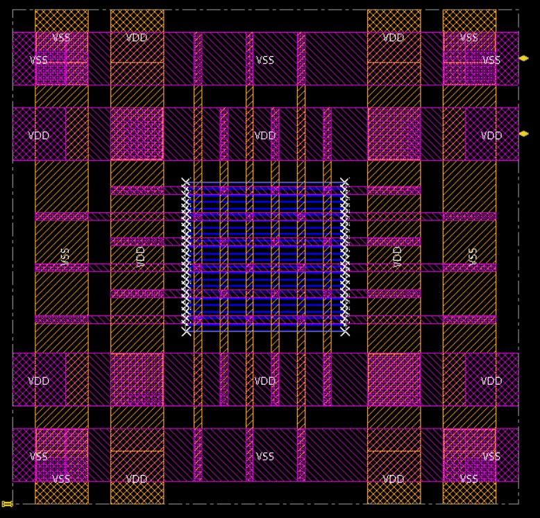
We can see the M1 stripes that we laid in for stdcells, as well as the power ring and its stripes. The power ring looks quite large compared to the previous tutorial, but the GCD unit is quite a small design, and we will eventually be connecting this design to a full pad ring in the chip flow, which will justify our power ring width choices.
Let’s run the bulk of the cadence flow, the pnr step. This is the step where we’ll actually do placement, clock-tree synthesis and optimization and routing. We also have the ability to add in setup and hold time fixing for designs that have violating paths. This step will likely take the longest. For a simple design like this one, however, it should be no more than a few minutes. For more complex designs, do not be surprised to see pnr take 30-45 minutes or even longer.
 % cd $TOPDIR/asic/build
 % make 9

 OR

 % make brg-cadence-innovus-pnr
The automated system is setup to output a bunch of reports in the reports directory.
This step does some pre-placement reporting, pre Clock-Tree Synthesis reporting, and
hold time reporting. Feel free to look at these reports, however in the signoff step
we will output many more reports that more accurately reflect your final design.
An important function of the pnr step is its ability to perform hold time fixing. In
the event that you push your design through the Innovus flow and move onto
Back-Annotated Gate-level simulation only to find that your design has hold time
violations, you will need to return back to this step and rebuild it. However, this
time, you will need to use a more strict hold time and setup time constraint. To do
this, you would need to update the parameters dictionary within
SortUnitStructRTL_BlockFlow.py to include the parameters setup_slack and
hold_slack. It is crucial that you include both of these parameters, otherwise you
risk hold time fixes causing violations in setup time. Then, in order to actually
rebuild the step properly, we will need to re-run the mflowgen run command we ran
earlier, because our flow.py file has been modified. Then we will need to run the
make-clean target on this step to remove its contents before rebuilding the step.
You will also need to rebuild every step after the pnr step using the same
make-clean-N make-N pattern.
 % mflowgen run --design ../../sim/tut3_pymtl/sort
 % make clean-9
 % make 9
If you’d like, you can take a look at the design.checkpoint the same way we did in the previous step.
 % cd $TOPDIR/asic/build/9-brg-cadence-innovus-pnr
 % innovus -64 -nolog
 % innovus> source checkpoints/design.checkpoint/save.enc
 % make 10
  OR
 % make brg-cadence-innovus-signoff
Let’s continue to signoff, where all of our important output files from the
innovus flow will be generated. Here is where we generate the .gds, .sdf,
.lef, .spef, the updated gate-level netlist from innovus, as well as the
final signoff timing, area, and power reports. Make sure to take a look at the
signoff reports. You might want to start with the timing summary, and hold
timing summary reports, which can be opened like this:
 % cd $TOPDIR/asic/build/10-brg-cadence-innovus-signoff/reports/innovus
 % less signoff.summary.gz
 ...

+--------------------+---------+---------+---------+---------+---------+---------+
|     Setup mode     |   all   | default | In2Out  | In2Reg  | Reg2Out | Reg2Reg |
+--------------------+---------+---------+---------+---------+---------+---------+
|           WNS (ns):|  0.118  |  0.000  |   N/A   |  0.486  |  0.124  |  0.118  |
|           TNS (ns):|  0.000  |  0.000  |   N/A   |  0.000  |  0.000  |  0.000  |
|    Violating Paths:|    0    |    0    |   N/A   |    0    |    0    |    0    |
|          All Paths:|   132   |    0    |   N/A   |   35    |   33    |   66    |
+--------------------+---------+---------+---------+---------+---------+---------+
 ...

 % cd $TOPDIR/asic/build/10-brg-cadence-innovus-signoff/reports/innovus
 % less signoff_hold.summary.gz
 ...
+--------------------+---------+---------+---------+---------+---------+---------+
|     Hold mode      |   all   | default | In2Out  | In2Reg  | Reg2Out | Reg2Reg |
+--------------------+---------+---------+---------+---------+---------+---------+
|           WNS (ns):|  0.020  |  0.000  |   N/A   |  0.020  |  0.161  |  0.093  |
|           TNS (ns):|  0.000  |  0.000  |   N/A   |  0.000  |  0.000  |  0.000  |
|    Violating Paths:|    0    |    0    |   N/A   |    0    |    0    |    0    |
|          All Paths:|   132   |    0    |   N/A   |   35    |   33    |   66    |
+--------------------+---------+---------+---------+---------+---------+---------+
...
Paths are organized into four groups: In2Reg, Reg2Out, In2Out, and Reg2Reg path groups. In2Reg paths start at an input port and end at a register; Reg2Out paths start at a register and end at an output port; In2Out paths start at an input port and end at an output port; and Reg2Reg paths start at a register and end at register. The following diagram is from Chapter 1 of the Synopsys Timing Constraints and Optimization User Guide.
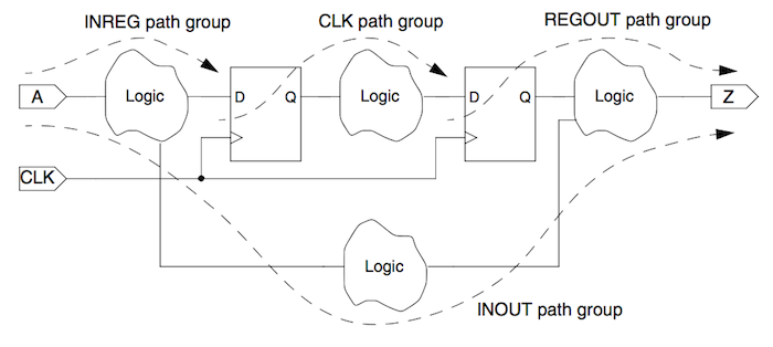
We have setup the flow so that the tools have to fit all four of these paths in a single cycle. The timing report shows the worst negative slack (WNS) and total negative slack (TNS) within each path group. The overall critical path for your design will be the worse critical path across all four groups. WNS is calculated as the the target clock minus the longest path. This is very important! If we have negative slack then the design must run slower than this clock constraint, and if we have positive slack then the design can run faster than this clock constraint. Again, the actual cycle time is the calculated by subtracting the WNS from the target clock period (and we must look across all four path groups to find the overall critical path). So in this example the Reg2Reg path group has the worst cycle time of 0.6 - 0.118 = 0.482ns.
Remember that hold time slack does not tell us anything about how quickly
we can run our design. A hold time violation is a result of the
contamination delay of a logical block being shorter than the hold time of
a particular flip-flop such that the data arrives too quickly following
a positive clock edge. Having a hold time violation simply means that you
will need to go back to the pnr step using a stricter hold_slack and
setup_slack so that buffers will be inserted to increase the contamination
delay of violating paths. If you do not fix your hold time violations,
your real design will not work, no matter how slow you run your design.
To figure out the actual critical path through the design you will need to look in the detailed timing report for each path group. These timing reports are organized such that the worst case path is shown first. This means you cannot just look at one timing report for a path group! The critical path might be in a different path group. So first, use the timing summary report to figure out which path group contains the critical path, and then look in the corresponding timing report to see the critical path like this:
 % cd $TOPDIR/asic/build/10-brg-cadence-innovus-signoff/reports/innovus
 % less signoff_Reg2Out.tarpt.gz
 ...
Path 1: MET Setup Check with Pin elm_S1S2__2/out_reg_5_/CK
Endpoint:   elm_S1S2__2/out_reg_5_/D (v) checked with  leading edge of 'ideal_
clock'
Beginpoint: elm_S0S1__3/out_reg_2_/Q (^) triggered by  leading edge of 'ideal_
clock'
Path Groups: {Reg2Reg}
Analysis View: analysis_default
Other End Arrival Time         -0.003
- Setup                         0.030
+ Phase Shift                   0.600
+ CPPR Adjustment               0.000
= Required Time                 0.567
- Arrival Time                  0.449
= Slack Time                    0.118
     Clock Rise Edge                      0.000
     + Drive Adjustment                   0.012
     + Source Insertion Delay            -0.077
     = Beginpoint Arrival Time           -0.065
     Timing Path:
     +----------------------------------------------------------------------------------------------------+
     |            Pin            | Edge |          Net           |   Cell    | Delay | Arrival | Required |
     |                           |      |                        |           |       |  Time   |   Time   |
     |---------------------------+------+------------------------+-----------+-------+---------+----------|
     | clk[0]                    |  ^   | clk[0]                 |           |       |  -0.065 |    0.053 |
     | CTS_ccl_a_buf_00010/A     |  ^   | clk[0]                 | CLKBUF_X3 | 0.001 |  -0.064 |    0.054 |
     | CTS_ccl_a_buf_00010/Z     |  ^   | CTS_4                  | CLKBUF_X3 | 0.063 |  -0.001 |    0.117 |
     | elm_S0S1__3/out_reg_2_/CK |  ^   | CTS_4                  | DFF_X1    | 0.001 |  -0.000 |    0.118 |
     | elm_S0S1__3/out_reg_2_/Q  |  ^   | elm_S0S1__out[2]       | DFF_X1    | 0.106 |   0.105 |    0.223 |
     | minmax1_S1/U17/A          |  ^   | elm_S0S1__out[2]       | INV_X1    | 0.000 |   0.105 |    0.223 |
     | minmax1_S1/U17/ZN         |  v   | minmax1_S1/n6          | INV_X1    | 0.008 |   0.113 |    0.231 |
     | minmax1_S1/U3/A2          |  v   | minmax1_S1/n6          | OR2_X1    | 0.000 |   0.113 |    0.231 |
     | minmax1_S1/U3/ZN          |  v   | minmax1_S1/n7          | OR2_X1    | 0.048 |   0.162 |    0.280 |
     | minmax1_S1/U18/B          |  v   | minmax1_S1/n7          | OAI211_X1 | 0.000 |   0.162 |    0.280 |
     | minmax1_S1/U18/ZN         |  ^   | minmax1_S1/n15         | OAI211_X1 | 0.023 |   0.184 |    0.302 |
     | minmax1_S1/U10/A1         |  ^   | minmax1_S1/n15         | AND3_X1   | 0.000 |   0.184 |    0.302 |
     | minmax1_S1/U10/ZN         |  ^   | minmax1_S1/n19         | AND3_X1   | 0.046 |   0.230 |    0.348 |
     | minmax1_S1/U23/C2         |  ^   | minmax1_S1/n19         | OAI211_X1 | 0.000 |   0.230 |    0.348 |
     | minmax1_S1/U23/ZN         |  v   | minmax1_S1/n23         | OAI211_X1 | 0.022 |   0.252 |    0.370 |
     | minmax1_S1/U7/A1          |  v   | minmax1_S1/n23         | AND2_X1   | 0.000 |   0.252 |    0.370 |
     | minmax1_S1/U7/ZN          |  v   | minmax1_S1/n29         | AND2_X1   | 0.033 |   0.286 |    0.404 |
     | minmax1_S1/U32/B1         |  v   | minmax1_S1/n29         | OAI21_X2  | 0.000 |   0.286 |    0.404 |
     | minmax1_S1/U32/ZN         |  ^   | minmax1_S1/n32         | OAI21_X2  | 0.098 |   0.384 |    0.502 |
     | minmax1_S1/U40/S          |  ^   | minmax1_S1/n32         | MUX2_X1   | 0.001 |   0.385 |    0.503 |
     | minmax1_S1/U40/Z          |  v   | minmax1_S1__out_min[5] | MUX2_X1   | 0.064 |   0.449 |    0.567 |
     | elm_S1S2__2/out_reg_5_/D  |  v   | minmax1_S1__out_min[5] | DFF_X1    | 0.000 |   0.449 |    0.567 |
     +----------------------------------------------------------------------------------------------------+
This report is similar to the timing reports you saw in the previous tutorial. Note that we can now see the clock network delay factored into the beginning of the path. For paths that start at a register and end at a register within the same design, we will see the clock network delay factored both at the beginning and end of the path. If these delays are not equal we will have either positive or negative clock skew. We have setup the tools so that these paths must also be completed within one cycle. For Reg2Out paths, there is no clock network delay at the end of the path, because the end point is an output port not a register. This might seem to penalize these REGOUT paths, but keep in mind that there will be a register in the next module which will have some setup time. So we will still end up with a reasonable estimate even for REGOUT paths. The fanout and parasitic capacitance on each net is also shown which can be useful in identifying nets with unusually high loads. This critical path is similar but not exactly the same as we saw in the previous tutorial. This is because the ASIC flow uses more commands with different options than what we did manually.
You can view the area report like this:
 % cd $TOPDIR/asic/build/10-brg-cadence-innovus-signoff/reports
 % less area.rpt
Hinst Name                 Module Name                                                    Inst Count           Total Area               Buffer             Inverter        Combinational                 Flop                Latch           Clock Gate                Macro             Physical
----------------------------------------------------------------------------------------------------------------------------------------------------------------------------------------------------------------------------------------------------------------------------------------------------------
SortUnitStructRTL__nbits_8                                                                       391              776.188                4.788               32.984              290.738              447.678                0.000                0.000                0.000                0.000
 elm_S0S1__0               SortUnitStructRTL__nbits_8_Reg__Type_Bits8_0                            8               36.176                0.000                0.000                0.000               36.176                0.000                0.000                0.000                0.000
 elm_S0S1__1               SortUnitStructRTL__nbits_8_Reg__Type_Bits8_11                           8               36.176                0.000                0.000                0.000               36.176                0.000                0.000                0.000                0.000
 elm_S0S1__2               SortUnitStructRTL__nbits_8_Reg__Type_Bits8_10                           8               36.176                0.000                0.000                0.000               36.176                0.000                0.000                0.000                0.000
 elm_S0S1__3               SortUnitStructRTL__nbits_8_Reg__Type_Bits8_9                            8               36.176                0.000                0.000                0.000               36.176                0.000                0.000                0.000                0.000
 elm_S1S2__0               SortUnitStructRTL__nbits_8_Reg__Type_Bits8_8                            8               36.176                0.000                0.000                0.000               36.176                0.000                0.000                0.000                0.000
 elm_S1S2__1               SortUnitStructRTL__nbits_8_Reg__Type_Bits8_7                            8               36.176                0.000                0.000                0.000               36.176                0.000                0.000                0.000                0.000
 elm_S1S2__2               SortUnitStructRTL__nbits_8_Reg__Type_Bits8_6                            8               36.176                0.000                0.000                0.000               36.176                0.000                0.000                0.000                0.000
 elm_S1S2__3               SortUnitStructRTL__nbits_8_Reg__Type_Bits8_5                            8               36.176                0.000                0.000                0.000               36.176                0.000                0.000                0.000                0.000
 elm_S2S3__0               SortUnitStructRTL__nbits_8_Reg__Type_Bits8_4                            8               36.176                0.000                0.000                0.000               36.176                0.000                0.000                0.000                0.000
 elm_S2S3__1               SortUnitStructRTL__nbits_8_Reg__Type_Bits8_3                            8               36.176                0.000                0.000                0.000               36.176                0.000                0.000                0.000                0.000
 elm_S2S3__2               SortUnitStructRTL__nbits_8_Reg__Type_Bits8_2                            8               36.176                0.000                0.000                0.000               36.176                0.000                0.000                0.000                0.000
 elm_S2S3__3               SortUnitStructRTL__nbits_8_Reg__Type_Bits8_1                            8               36.176                0.000                0.000                0.000               36.176                0.000                0.000                0.000                0.000
 minmax0_S1                SortUnitStructRTL__nbits_8_MinMaxUnit__nbits_8_0                       49               56.924                0.000                5.852               51.072                0.000                0.000                0.000                0.000                0.000
 minmax0_S2                SortUnitStructRTL__nbits_8_MinMaxUnit__nbits_8_4                       50               57.722                0.000                6.384               51.338                0.000                0.000                0.000                0.000                0.000
 minmax1_S1                SortUnitStructRTL__nbits_8_MinMaxUnit__nbits_8_3                       50               57.456                0.000                6.384               51.072                0.000                0.000                0.000                0.000                0.000
 minmax1_S2                SortUnitStructRTL__nbits_8_MinMaxUnit__nbits_8_2                       49               56.924                0.000                5.852               51.072                0.000                0.000                0.000                0.000                0.000
 minmax_S3                 SortUnitStructRTL__nbits_8_MinMaxUnit__nbits_8_1                       52               55.860                0.000                6.916               48.944                0.000                0.000                0.000                0.000                0.000
 val_S0S1                  SortUnitStructRTL__nbits_8_RegRst__Type_Bits1__reset_value_0_0          3                6.118                0.000                0.532                1.064                4.522                0.000                0.000                0.000                0.000
 val_S1S2                  SortUnitStructRTL__nbits_8_RegRst__Type_Bits1__reset_value_0_2          3                6.118                0.000                0.532                1.064                4.522                0.000                0.000                0.000                0.000
 val_S2S3                  SortUnitStructRTL__nbits_8_RegRst__Type_Bits1__reset_value_0_1          3                6.118                0.000                0.532                1.064                4.522                0.000                0.000                0.000                0.000
This report is similar to what we saw in the previous tutorial. Note that the total cell area is different from the total core area. The total cell area includes just the standard cells, while the total area includes the “Net Interconnect Area”. To be totally honest, I am not quite sure what “Net Interconnect Area” actually means, but we use the total core area in our analysis. Again these numbers are not identical to the previous tutorial, since the ASIC flow uses more commands with different options than what we did manually.
We have written a little script to parse the reports and generate a
summary.txt file. This script takes care of looking across all four
path groups to fine the true cycle time that you should use in your
analysis. Note here that the ‘chip_area’ is quite large, but recall
that this is including our power rails, and will look more natural
with bigger and more complex designs, the key area point to see here
is the core_area which capture stdcell area, macro area, and
net interconnect area.
 % cd $TOPDIR/asic/build/10-brg-cadence-innovus-signoff/reports
 % less summary.txt

==========================================================================
  Summary
==========================================================================

design_name = SortUnitStructRTL__nbits_8

area & timing
  design_area   = 857.584 um^2
  stdcells_area = 857.584 um^2
  macros_area   = 0.0 um^2
  chip_area     = 11736.346 um^2
  core_area     = 1113.476 um^2
  constraint    = 0.6 ns
  slack         = 0.117 ns
  actual_clk    = 0.483 ns
While we do not use GUIs to drive our flow, we often use GUIs to analyze the results. You can start the Cadence Innovus GUI to visualize the final layout like this:
 % cd $TOPDIR/asic/build/10-brg-cadence-innovus-signoff
 % innovus -64
 % innovus> source checkpoints/design.checkpoint/save.enc
As mentioned in the previous tutorial, we call the resulting plot an “amoeba plot” because the tool often generates blocks that look like amoebas. You can zoom in to see how the standard cells were placed and how the routing was done. You can turn on an off the visibility of metal layers using the panel on the right. One very useful feature is to view the hierarchy and area breakdown. This will be critical for producing high-quality amoeba plots. You can use the following steps to highlight various modules on the amoeba plot:
- Choose Windows > Workspaces > Design Browser + Physical from the
- menu Hide all of the metal layers by pressing the number keys Browse
- the design hierarchy using the panel on the left Right click on a
- module, click Highlight, select a color
Another very useful feature is to highlight the critical path on the amoeba plot using the following steps:
- Choose Timing > Debug Timing from the menu
- Click OK in the pop-up window
- Right click on first path in the Path List
- Choose Highlight > Only This Path > Color
You can see an example amoeba plot below. Note that you will need to use some kind of “screen-capture” software to capture the plot. You will also need to play with the colors to enable easily seeing the various parts of your design.
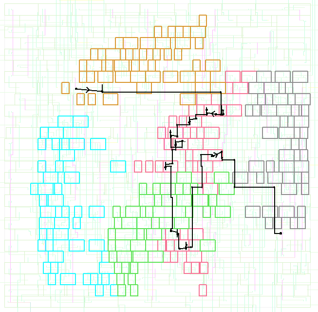
Using Synopsys VCS for Back-Annotated Gate-Level Simulation
We are now prepared to use the .sdf we just generated from innovus to
run a series of Back-Annotated Gate-Level simulations that will give us
insight into realistic timing characteristics of our design. Remember,
we have configured the same VCS-sim to back-annotated gate-level simulation
by simply including an sdf file at the input, and we include the innovus
gate-level netlist, which has been updated to include any new cells that
may have been added by innovus during timing optimization/hold-time fixing.
Feel free to run the info target for this step to see for yourself how
everything is configured. We run the step just as the previous two VCS
simulations:
 % cd $TOPDIR/asic/build
 % make 11
 OR
 % make PostPNR-Gate-Level-Simulation
 ...
 [FAILED]: test_basic
 [FAILED]: test_stream
 [FAILED]: test_dups
 [FAILED]: test_sorted
 [FAILED]: test_random_8
 [FAILED]: sort-rtl-struct-random
 [FAILED]: sort-rtl-struct-sorted-fwd
 [FAILED]: sort-rtl-struct-sorted-rev
 [FAILED]: sort-rtl-struct-zeros
 === Ending Simulations ================
Uh oh! We failed Back-Annotated Gate-Level simulation! Let’s take a look at the simplest test’s report file to see if we can figure out what’s going wrong.
 % cd $TOPDIR/asic/build/10-PostPNR-Gate-Level-Simulation/reports
 % less test_basic.rpt
 ...
 "./inputs/adk/stdcells.v", 2123: Timing violation in SortUnitStructRTL__nbits_8_tb.DUT.val_S0S1.out_reg_0_
    $setuphold( posedge CK:2166, negedge D:2178, limits: (29,15) );


 "./inputs/adk/stdcells.v", 2124: Timing violation in SortUnitStructRTL__nbits_8_tb.DUT.val_S0S1.out_reg_0_
     $setuphold( posedge CK:2766, posedge D:2758, limits: (29,15) );


 The test bench received a value containing X/Z's! Please note
 that the VTB is pessmistic about X's and you should make sure
 all output ports of your DUT does not produce X's after reset.
 - Timestamp      : 4 (default unit: ns)
 - Cycle number   : 5 (variable: cycle_count)
 - line number    : line 4 in SortUnitStructRTL__nbits_8_test_basic_tb.v.cases
 - port name      : out[0] (out[0] in Verilog)
 - expected value : 0x00
 - actual value   : 0x0X
We can see two timing violations reported by vcs before we actually get to the check which caused the testbench to fail. The first timing violation says that the clk edge is at 2166ps, but data changes at 2178ps, or 12ps after the clk. The hold time for this flip-flop is 15ps. Therefore, it is likely that we have violated a hold time constraint, although it is possible that we have just severely violated setup time such that the data is 29+12 = 41ps late. There are a few different ways we can check this, but I think one of the easiest ways to diagnose problems with back-annotated gate-level simulations is to compare the waveforms with a passing fast-functional gate-level simulation. Debugging this way is very useful because the fast-functional simulation is almost like the “answer key” to what the signals should be in a given cycle. This makes it easier to distinguish setup violations from hold violations. Let’s setup two waveform windows using gtkwave to analyze this problem.
 % cd $TOPDIR/asic/build/10-PostPNR-Gate-Level-Simulation/outputs/vcd
 % gtkwave test_basic.vcd &
 % cd $TOPDIR/asic/build/5-PostSynth-Gate-Level-Simulation/outputs/vcd
 % gtkwave test_basic.vcd &
The violating path went to the flip flop out_reg_0 inside the val_S0S1
module. In both gtkwave windows, open up the clk signal, the data bit of
out_reg_0 and the Q bit of out_reg_0. The resulting waveform for the
fast functional simulation should look like this:
And the Back Annotated simulation should look like this:
Aha! If you zoom in near the portion of the waveform where the timing
violation occurs, we can see clearly from the fast functional waveform
that the valid bit is supposed to change after the clock. Therefore,
this is a hold time violation. This makes sense, the val_S0S1 register
connects directly to an input in_val. Input registered paths are the
most likely to be affected by hold time constraints in simulation,
because we the user tell the simulation when the data is arriving from
externally, since we do not know what logic lies beyond our current
design. To fix this, we will need to insert buffers into the violating
path so that it will meet the hold time. To do this we must edit the
SortUnitStructRTL_BlockFlow.py file, and go back to the PNR step.
Performing Hold Fixing on a Design
In order to actually fix the hold time violations, we will need to enforce
a stricter hold time constraint on the design in the pnr step. To do this,
we will need to rebuild that step and all subsequent steps. We will also
need to update the SortUnitStructRTL_BlockFlow.py file to tell the flow
what hold time constraint to use. Open up the flow.py file using vim,
geany, vscode, or your favorite text editor. In the parameters dictionary,
add the following lines:
    # Hold Fixing
    'hold_slack'      : 0.070,
    'setup_slack'     : 0.035,
These numbers should work, but in your own designs you may need to do some trial and error to see what works best for your design. Now that we’ve updated the flow.py file, let’s reconstruct mflowgen, and clean the necessary steps that need to be rebuilt.
 % mflowgen run --design ../../sim/tut3_pymtl/sort
 % make clean-9
 % make clean-10
 % make clean-11
We clean all the steps we did after pnr, since they will need to be rebuilt. Now let’s build pnr again:
% make 9
Look to the run.log in the logs directory of the step to see what’s changed.
Ctrl+F for *** Finished Core Fixing and below that you should find a little
summary that tells you how many cells were added for hold time fixing:
*** Finished Core Fixing (fixHold) cpu=0:00:01.7 real=0:00:02.0 totSessionCpu=0:00:58.8 mem=1521.9M density=77.019% ***

*info:
*info: Added a total of 102 cells to fix/reduce hold violation
*info:
*info: Summary:
*info:          102 cells of type 'BUF_X1' used
This is a good sanity check to make sure that we actually changed something about the netlist, if we use too loose of a constraint, innovus could still exit claiming that no hold time fixing was needed.
Now, let’s rebuild both signoff and Back-Annotated Sim.
 % make 10
 % make 11
 ...
 [PASSED]: test_basic
 [PASSED]: test_stream
 [PASSED]: test_dups
 [PASSED]: test_sorted
 [PASSED]: test_random_8
 [PASSED]: sort-rtl-struct-random
 [PASSED]: sort-rtl-struct-sorted-fwd
 [PASSED]: sort-rtl-struct-sorted-rev
 [PASSED]: sort-rtl-struct-zeros
 === Ending Simulations ================
Great! We fixed the hold time violations, and now we can move on to power analysis.
Using Synopsys PrimeTime for Post-Place-and-Route Power Analysis
Earlier in this tutorial we utilized Synopsys PrimeTime to do power
analysis at the Post-Synthesis stage of the flow. This provides a quick
and dirty way to get power estimates on our design, but the
Post-Place-and-Route power analysis will be much more accurate, since we
will have the final netlist as well as a .spef file that can take into
consideration the actual routing done between stdcells.
 % cd $TOPDIR/asic/build
 % make 12
 OR
 % make PostPNR-power-analysis
Similarly, this step outputs summary information, but also a power report and power hierarchy report. Feel free to open these files up to take a look and compare it to the power and energy from the Post-Synth energy analysis.
These results are similar to what we saw in the previous tutorial.
Reviewing the Flow Summary
We have also created a simple flow summary step which collects the summary reports from Innovus signoff and Synopsys PT power analysis steps and puts them into one file thats easy to read. Let’s run the flow summary here:
 % cd $TOPDIR/asic/build
 % make 13
 OR
 % make brg-flow-summary
 ...
==========================================================================
  Summary
==========================================================================

design_name = SortUnitStructRTL__nbits_8

area & timing
  design_area   = 857.584 um^2
  stdcells_area = 857.584 um^2
  macros_area   = 0.0 um^2
  chip_area     = 11736.346 um^2
  core_area     = 1113.476 um^2
  constraint    = 0.6 ns
  slack         = 0.117 ns
  actual_clk    = 0.483 ns


==========================================================================
 Fast-Functional Power Analysis
==========================================================================

 power & energy
  sort-rtl-struct-random.vcd
      exec_time = 106 cycles
      power     = 2.367 mW
      energy    = 0.150541 nJ

  sort-rtl-struct-sorted-fwd.vcd
      exec_time = 106 cycles
      power     = 2.245 mW
      energy    = 0.142782 nJ

  sort-rtl-struct-sorted-rev.vcd
      exec_time = 106 cycles
      power     = 2.196 mW
      energy    = 0.139666 nJ

  sort-rtl-struct-zeros.vcd
      exec_time = 106 cycles
      power     = 1.161 mW
      energy    = 0.0738396 nJ

==========================================================================
 Back-Annotated Power Analysis
==========================================================================

 power & energy
  sort-rtl-struct-random.vcd
      exec_time = 106 cycles
      power     = 3.099 mW
      energy    = 0.197096 nJ

  sort-rtl-struct-sorted-fwd.vcd
      exec_time = 106 cycles
      power     = 2.817 mW
      energy    = 0.179161 nJ

  sort-rtl-struct-sorted-rev.vcd
      exec_time = 106 cycles
      power     = 2.724 mW
      energy    = 0.173246 nJ

  sort-rtl-struct-zeros.vcd
      exec_time = 106 cycles
      power     = 1.454 mW
      energy    = 0.0924744 nJ
While the summary report is a great tool to get quick overview of your design, do be sure to dig into the other reports to verify that your design is working as you expect.
Using Verilog RTL Models
Students are welcome to use Verilog instead of PyMTL3 to design their RTL models. Having said this, we will still exclusively use PyMTL3 for all test harnesses, FL/CL models, and simulation drivers. This really simplifies managing the course, and PyMTL3 is actually a very productive way to test/evaluate your Verilog RTL designs. We use PyMTL3’s Verilog import feature described in the Verilog tutorial to make all of this work. The following commands will run all of the tests on the Verilog implementation of the sort unit.
 % cd $TOPDIR/sim/build
 % rm -rf *
 % pytest ../tut4_verilog/sort
 % pytest ../tut4_verilog/sort --test-verilog --dump-vtb
As before, the tests for the SortUnitStructRTL will fail. You can just
copy over your implementation of the MinMaxUnit from when you completed
the Verilog tutorial. If you have not completed the Verilog tutorial then
you might want to go back and do that now. Basically the MinMaxUnit
should look like this:
`ifndef TUT4_VERILOG_SORT_MIN_MAX_UNIT_V
`define TUT4_VERILOG_SORT_MIN_MAX_UNIT_V

module tut4_verilog_sort_MinMaxUnit
#(
  parameter p_nbits = 1
)(
  input  logic [p_nbits-1:0] in0,
  input  logic [p_nbits-1:0] in1,
  output logic [p_nbits-1:0] out_min,
  output logic [p_nbits-1:0] out_max
);

  always_comb begin

    // Find min/max

    if ( in0 >= in1 ) begin
      out_max = in0;
      out_min = in1;
    end
    else if ( in0 < in1 ) begin
      out_max = in1;
      out_min = in0;
    end

    // Handle case where there is an X in the input

    else begin
      out_min = 'x;
      out_max = 'x;
    end

  end

endmodule

`endif /* TUT4_VERILOG_SORT_MIN_MAX_UNIT_V */
After running the tests we use the sort unit simulator to translate the Verilog RTL model into Verilog and to dump the VTB file that we want to use for VCS.
 % cd $TOPDIR/sim/build
 % ../tut4_verilog/sort/sort-sim --impl rtl-struct --stats --translate --dump-vtb
Take a moment to open up the translated Verilog which should be in a file
named SortUnitFlatRTL__nbits_8__pickled.v. You might ask, “Why do we
need to use PyMTL3 to translate the Verilog if we already have the
Verilog?” PyMTL3 will take care of preprocessing all of your Verilog RTL
code to ensure it is in a single Verilog file. This greatly simplifies
getting your design into the ASIC flow. This also ensures a one-to-one
match between the Verilog that was used to generate the VCD file and the
Verilog that is used in the ASIC flow.
Once you have tested your design and generated the single Verilog file and the VCD file, you can push the design through the ASIC flow using mflowgen like this:
 % mkdir -p $TOPDIR/asic/build-verilog
 % cd $TOPDIR/asic/build-verilog
 % mflowgen run --design ../../sim/tut4_verilog/sort
 % make
The PyMTL RTL and Verilog RTL designs should show similar results, but obviously they won’t be exactly the same since the source code is different. Make sure to go through all of the reports to make sure that your design got through thr flow properly.
To Do On Your Own
Use what you have learned so far to push the GCD Unit through the flow.
You can use either the PyMTL3 or Verilog GCD Unit provided along with
this tutorial. You will need to verify the GCD Unit works, and generate the
corresponding Verilog RTL using the GCD Unit simulator. Use the provided
tut6_flow_gcd.py file along with PyHFlow to push the design through the
flow.