ECE 5745 Tutorial 9: TinyRV2 Accelerators
- Author: Christopher Batten, Jack Brzozowski
- Date: March 23, 2021
Table of Contents
- Introduction
- Baseline TinyRV2 Processor FL and RTL Models
- Cross-Compiling and Executing TinyRV2 Microbenchmarks
- TinyRV2 Processor ASIC
- VVADD Accelerator FL, CL, and RTL Models
- VVADD Accelerator ASIC
- Integrating the TinyRV2 Processor and the VVADD Accelerator
- Accelerating a TinyRV2 Microbenchmark
- TinyRV2 Processor + VVADD Accelerator ASIC
- Using Verilog Accelerator RTL Models
Introduction
The infrastructure for the ECE 5745 lab assignments and projects has support for implementing medium-grain accelerators. Fine-grain accelerators are tightly integrated within the processor pipeline (e.g., a specialized functional unit for bit-reversed addressing useful in implementing an FFT), while coarse-grain accelerators are loosely integrated with a processor through the memory hierarchy (e.g., a graphics rendering accelerator sharing the last-level cache with a general-purpose processor). Medium-grain accelerators are often integrated as co-processors: the processor can directly send/receive messages to/from the accelerator with special instructions, but the co-processor is relatively decoupled from the main processor pipeline and can also independently interact with memory.
This tutorial will use the vector-vector-add (vvadd) microbenchmark as an example. We will explore the area and timing of a baseline TinyRV2 pipelined processor and the energy and performance when this processor is used to execute a pure-software version of the vvadd microbenchmark. We will then implement a vvadd accelerator, integrate it with the TinyRV2 pipelined processor, and determine the potential benefit of hardware acceleration for this simple microbenchmark. This tutorial assumes you have already completed the tutorials on Linux, Git, PyMTL, Verilog, the Synopsys ASIC tools, the PyHFlow automated ASIC flow, and SRAM generators.
The first step is to source the setup script, clone this repository from GitHub, and define an environment variable to keep track of the top directory for the project.
 % source setup-ece5745.sh
 % mkdir -p $HOME/ece5745
 % cd $HOME/ece5745
 % git clone git@github.com:cornell-ece5745/ece5745-tut9-xcel
 % cd ece5745-tut9-xcel
 % TOPDIR=$PWD
Baseline TinyRV2 Processor FL and RTL Models
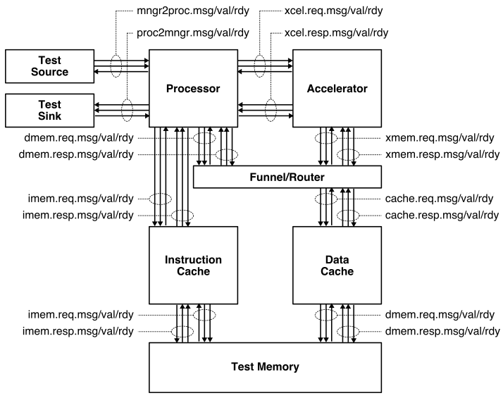
The following figure illustrates the overall system we will be using with our TinyRV2 processors. The processor includes eight latency insensitive val/rdy interfaces. The mngr2proc/proc2mngr interfaces are used for the test harness to send data to the processor and for the processor to send data back to the test harness. The imem master/minion interface is used for instruction fetch, and the dmem master/minion interface is used for implementing load/store instructions. The system includes both instruction and data caches. The xcel master/minion interface is used for the processor to send messages to the accelerator. The mngr2proc/proc2mngr and memreq/memresp interfaces were all introduced in ECE 4750. For now we will largely ignore the accelerator, and we will defer discussion of the xcel master/minion interfaces to later in this tutorial.
We provide two implementations of the TinyRV2 processor. The FL model in
sim/proc/ProcFL.py is essentially an instruction-set-architecture (ISA)
simulator; it simulates only the instruction semantics and makes no
attempt to model any timing behavior. As a reminder, the TinyRV2
instruction set is defined here:
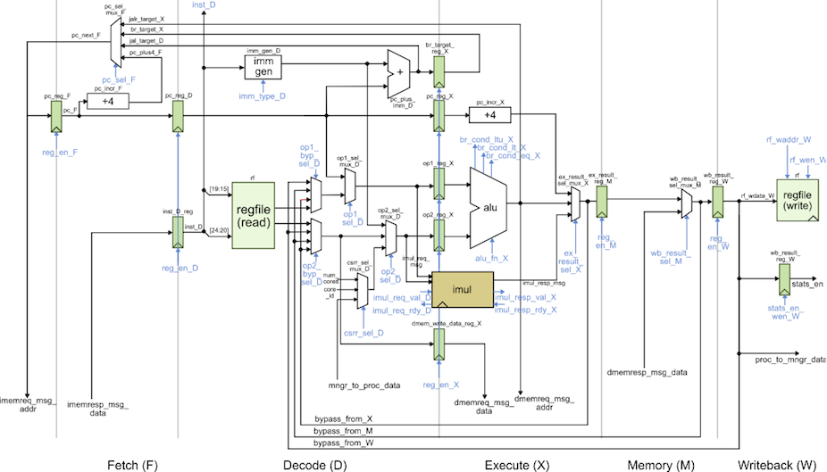
The RTL model in sim/proc/ProcPRTL.py is similar to the alternative
design for lab 2 in ECE 4750. It is a five-stage pipelined processor that
implements the TinyRV2 instruction set and includes full
bypassing/forwarding to resolve data hazards. There are two important
differences from the alternative design for lab 2 of ECE 4750. First, the
new processor design uses a single-cycle integer multiplier. We can push
the design through the flow and verify that the single-cycle integer
multiplier does not adversely impact the overall processor cycle time.
Second, the new processor design includes the ability to handle new CSRs
for interacting with medium-grain accelerators. The datapath diagram for
the processor is shown below.
We should run all of the unit tests on both the FL and RTL processor models to verify that we are starting with a working processor.
 % mkdir -p $TOPDIR/sim/build
 % cd $TOPDIR/sim/build
 % pytest ../proc
 % pytest ../proc --test-verilog
See the handout for lab 2 from ECE 4750 for more information about how we
use pytest and the mngr2proc/proc2mngr interfaces to test the TinyRV2
processor.
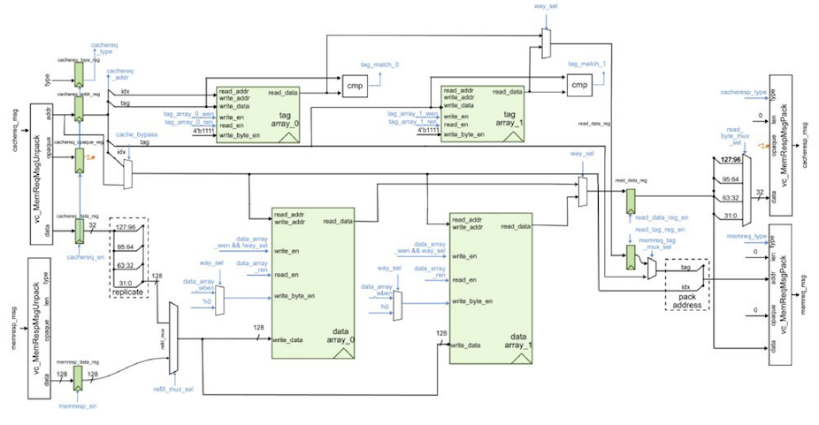
We also provide an RTL model in sim/cache/BlockingCachePRTL.py which is
very similar to the alternative design for lab 3 of ECE 4750. It is a
two-way set-associative cache with 16B cache lines and a
write-back/write-allocate write policy and LRU replacement policy. There
are three important differences from the alternative design for lab 3 of
ECE 4750. First, the new cache design is larger with a total capacity of
8KB. Second, the new cache design carefully merges states to enable a
single-cycle hit latency for both reads and writes. Note that writes have
a two cycle occupancy (i.e., back-to-back writes will only be able to be
serviced at half throughput). Third, the previous cache design used
combinational-read SRAMs, while the new cache design uses
synchronous-read SRAMs. Combinational-read SRAMs mean the read data is
valid on the same cycle we set the read address. Synchronous-read SRAMs
mean the read data is valid on the cycle after we set the read address.
Combinational SRAMs simplify the design, but are not realistic. Almost
all real SRAM memory generators used in ASIC toolflows produce
synchronous-read SRAMs, and indeed the CACTI memory compiler discussed in
the previous tutorial also produces synchronous-read SRAMs. Using
synchronous-read SRAMs requires non-trivial changes to both the datapath
and the control logic. The cache FSM must make sure all control signals
for the SRAM are ready the cycle before we need the read data. The
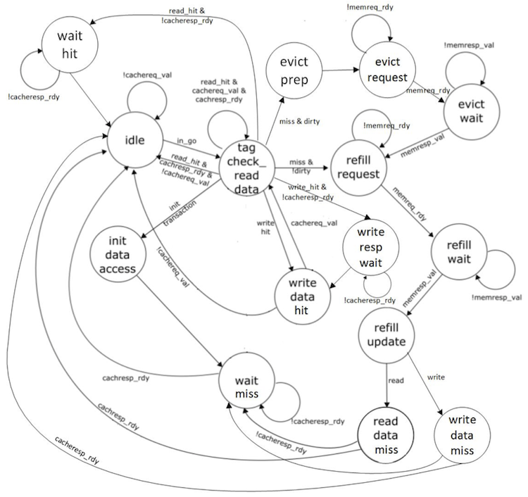
datapath and FSM diagrams for the new cache are shown below. Notice in
the FSM how we are able to stay in the TAG_CHECK_READ_DATA state if
another request is ready.
We should run all of the unit tests on the cache RTL model to verify that
we are starting with a working cache, and we should also use the
--test-verilog option to ensure the translated Verilog is correct.
 % mkdir -p $TOPDIR/sim/build
 % cd $TOPDIR/sim/build
 % pytest ../cache
 % pytest ../cache --test-verilog
Cross-Compiling and Executing TinyRV2 Microbenchmarks
We will write our microbenchmarks in C. Take a closer look at the vvadd
function which is located in app/ubmark/ubmark-vvadd.c:
 __attribute__ ((noinline))
 void vvadd_scalar( int *dest, int *src0, int *src1, int size )
 {
   for ( int i = 0; i < size; i++ )
     dest[i] = src0[i] + src1[i];
 }
We then have a set of tests that call this function and check to make
sure it produces the right results. You can see an example test in
app/ubmark/ubmark-vvadd-test1.c:
 void test_size3()
 {
   wprintf(L"test_size3\n");

   int src0[3] = { 1, 2, 3 };
   int src1[3] = { 4, 5, 6 };
   int dest[3] = { 0, 0, 0 };
   int ref[3]  = { 5, 7, 9 };

   vvadd_scalar( dest, src0, src1, 3 );

   for ( int i = 0; i < 3; i++ ) {
     if ( !( dest[i] == ref[i] ) )
       test_fail( i, dest[i], ref[i] );
   }
 }

 ...
 int main( int argc, char* argv[] )
 {
   test_size3();
   test_size8();
   test_pass();
   return 0;
 }
Some simple test functions such as test_fail and test_pass are
provided in app/common/common.h. We have a build system that can
compile these tests natively for x86 and can also cross-compile these
tests for TinyRV2 so they can be executed on our simulators. When
developing and testing microbenchmarks, we should always try to compile
them natively to ensure the microbenchmark is functionally correct before
we attempt to cross-compile the microbenchmark for TinyRV2. Debugging a
microbenchmark natively is much easier compared to debugging a
microbenchmark on our simulators. Here is how we compile and execute the
pure-software vvadd test natively:
 % mkdir -p $TOPDIR/app/build-native
 % cd $TOPDIR/app/build-native
 % ../configure
 % make ubmark-vvadd-test1
 % ./ubmark-vvadd-test1
The test should display passed. Once you are sure your test is working
correctly natively, you can cross-compile the test for TinyRV2.
 % mkdir -p $TOPDIR/app/build
 % cd $TOPDIR/app/build
 % ../configure --host=riscv32-unknown-elf
 % make ubmark-vvadd-test1
This will create a ubmark-vvadd-test1 binary which contains TinyRV2
instructions and data. You can disassemble a TinyRV2 binary (i.e., turn a
compiled binary back into an assembly text representation) with the
riscv32-objdump command like this:
 % cd $TOPDIR/app/build
 % riscv32-objdump ubmark-vvadd-test1 | less
 00000604 <vvadd_scalar(int*, int*, int*, int)>:
   604:  bge   x0,  x13, 630
   608:  slli  x13, x13, 0x2
   60c:  add   x13, x11, x13
   610:  lw    x15, 0(x11)   # <-.
   614:  lw    x14, 0(x12)   #   |
   618:  addi  x11, x11, 4   #   |
   61c:  addi  x12, x12, 4   #   |
   620:  add   x15, x15, x14 #   |
   624:  sw    x15, 0(x10)   #   |
   628:  addi  x10, x10, 4   #   |
   62c:  bne   x11, x13, 610 # --'
   630:  jalr  x0,  x1,  0
Recall that you can search with less by simply pressing the forward
slash key and typing in your search term. So you can find the assembly
code for the vvadd_scalar function by using less to search for
vvadd_scalar. You can also redirect the output from riscv32-objdump
to a text file for viewing with your favorite text editor. The
disassembly shows the address, bytes, and assembly text for each
instruction in the binary.
The assembly code for the vvadd_scalar function is similar to what we
saw in ECE 4750 although with some additional optimizations. I have added
some comments to show the backwards branch for the vvadd loop. The loop
has eight instructions. Four instructions do useful work (i.e., two LW
instructions, the actual ADDU instruction, one SW instruction) and three
ADDI instructions generate the array addresses by bumping the array
pointers. Notice that there is no explicit loop counter. The compiler has
instead calculated the address of one past the last element in the first
source array, and placed this value in x13. Each iteration, the BNE
instruction compares the current pointer to see if we have reached the
end of the array.
We have provided you with a simulator that composes a processor, cache, memory, and accelerator and is capable of executing TinyRV2 binaries. The simulator enables flexibly choosing the processor implementation (FL vs. RTL), the cache implementation (no cache vs. RTL), and the type and implementation of the accelerator. By default, the simulator uses the processor FL model, no cache model, and a null accelerator which we will discuss later. So let’s execute the vvadd test on the instruction-set simulator:
 % cd $TOPDIR/sim/build
 % ../pmx/pmx-sim ../../app/build/ubmark-vvadd-test1
After a few seconds the simulator should display passed which means the
test successfully executed on the ISA simulator. Now that we know that
our vvadd function is correct, we can start to evaluate its performance
using an evaluation program which serves as the actual microbenchmark.
Take a look at the microbenchmark in app/ubmark/ubmark-vvadd-eval.c:
 ...
 int main( int argc, char* argv[] )
 {
   int dest[size];

   for ( int i = 0; i < size; i++ )
     dest[i] = 0;

   test_stats_on();
   vvadd_scalar( dest, src0, src1, size );
   test_stats_off();

   for ( int i = 0; i < size; i++ ) {
     if ( !( dest[i] == ref[i] ) )
       test_fail( i, dest[i], ref[i] );
   }
   return 0;
 }
The src0, src1, and ref arrays are all defined in the
app/ubmark/ubmark-vvadd.dat file. The microbenchmark first initializes
the destination array to be all zeros, turns stats on, does the actual
vvadd computation, turns stats off, and finally verifies that the results
are as expected. We need the test_stats_on() and test_stats_off()
functions to make sure we can keep track of various statistics (e.g., the
number of cycles) only during the important part of the microbenchmark.
We do not want to count time spent in initialization or verification when
comparing the performance of our various microbenchmarks. These two
functions are defined in app/common/common-misc.h as follows:
 inline void test_stats_on()
 {
   int status = 1;
   asm( "csrw 0x7c1, %0" :: "r" (status) )
 }

 inline void test_stats_on()
 {
   int status = 0;
   asm( "csrw 0x7c1, %0" :: "r" (status) )
 }
We are using the GCC inline assembly extensions to enable us to directly insert a specific assembly instruction into our C code. You can find out more about inline assembly syntax here:
At a high level, %0 acts as a place holder for whatever register
specifier the compiler ends up allocating for the status variable. The
TinyRV2 instruction set defines CSR number 0x7c1 as the stats_en
control/status register, which is why we use 0x7c1 in the inline
assembly. Refer to the TinyRV2 instruction set for a list of the CSRs.
The idea is that the microarchitecture and/or simulator can monitor for
writes to the stats_en register to determine when to start and stop
keeping statistics. For more on writing microbenchmarks, please review
the handout for lab 5 from ECE 4750.
Before cross-compiling and analyzing this microbenchmark on our TinyRV2 processor, we always want to check that it works natively.
 % cd $TOPDIR/app/build-native
 % make ubmark-vvadd-eval
 % ./ubmark-vvadd-eval
The microbenchmark should display passed. Once you are sure your
microbenchmark is working correctly natively, you can cross-compile the
microbenchmark for TinyRV2.
 % mkdir -p $TOPDIR/app/build
 % cd $TOPDIR/app/build
 % ../configure --host=riscv32-unknown-elf
 % make ubmark-vvadd-eval
This will create a ubmark-vvadd-eval binary which contains TinyRV2
instructions and data. As with the test, you can disassemble a TinyRV2
binary with the riscv32-objdump command like this:
 % cd $TOPDIR/app/build
 % riscv32-objdump ubmark-vvadd-eval | less
 000002c0 <vvadd_scalar(int*, int*, int*, int)>:
    2c0:  bge   x0,  x13, 2ec
    2c4:  slli  x13, x13, 0x2
    2c8:  add   x13, x11, x13
    2cc:  lw    x15, 0(x11)   # <-.
    2d0:  lw    x14, 0(x12)   #   |
    2d4:  addi  x11, x11, 4   #   |
    2d8:  addi  x12, x12, 4   #   |
    2dc:  add   x15, x15, x14 #   |
    2e0:  sw    x15, 0(x10)   #   |
    2e4:  addi  x10, x10, 4   #   |
    2e8:  bne   x11, x13, 2cc # --'
    2ec:  jalr  x0,  x1, 0

 00000330 <main>:
    ...
    374:  sw    x0,  0(x15)               # <-. initialize
    378:  addi  x14, x14, 1               #   | dest
    37c:  addi  x15, x15, 4               #   | array
    380:  bne   x13, x14, 374             # --'
    384:  addi  x15, x0, 1
    388:  csrw  0x7c1, x15                # turn stats on
    38c:  addi  x18, x0, 1168             #
    390:  addi  x11, x18, 400             #
    394:  addi  x12, x0, 1168             #
    398:  addi  x10, x9, 0                #
    39c:  jal   x1,  2c0 <vvadd_scalar()> # call vvadd_scalar
    3a0:  addi  x15, x0, 0                #
    3a4:  csrw  0x7c1, x15                # turn stats off
    3a8:  lw    x11, -1728(x19)
    3ac:  bge   x0,  x11, 3f0 <main+0xc0>
    ...
You can see the CSRW instructions to set and clear the stats_en bit
have been inserted in the main function around the call to
vvadd_scalar. Now let’s verify that the microbenchmark produces the
right answer on the instruction-set simulator:
 % cd $TOPDIR/sim/build
 % ../pmx/pmx-sim ../../app/build/ubmark-vvadd-eval
After a few seconds the simulator should display passed which means the
microbenchmark successfully executed on the ISA simulator. The --trace
command line option will display each instruction as it is executed on
the ISA simulator.
 % cd $TOPDIR/sim/build
 % ../pmx/pmx-sim --trace ../../app/build/ubmark-vvadd-eval > ubmark-vvadd-fl.trace
When dumping out large line traces, it is usually much faster to save
them to a file and then open the file in your favorite text editor. You
can search in the line trace for the CSRW instruction to quickly jump to
where the actual vvadd_scalar function starts executing. Here is what
the line trace looks like for one iteration of the vvadd loop:
       PC       instruction           imemreq           imemresp          dmemreq                   dmemresp
----------------------------------------------------------------------------------------------------------------------
1671: -#                             |                 |                  rd:00:00000624:0:        |
1672: -#                             |                 |                                           |rd:00:0:0:00000000
1673: -000002d0 lw   x15, 0x000(x11) |                 |                                           |
1674: -#                             |rd:00:000002d0:0:|                                           |
1675: -#                             |                 |rd:00:0:0:00062703                         |
1676: -#                             |                 |                  rd:00:00000494:0:        |
1677: -#                             |                 |                                           |rd:00:0:0:00000047
1678: -000002d4 lw   x14, 0x000(x12) |                 |                                           |
1679: -#                             |rd:00:000002d4:0:|                                           |
1680: -#                             |                 |rd:00:0:0:00458593                         |
1681: -000002d8 addi x11, x11, 0x004 |                 |                                           |
1682: -#                             |rd:00:000002d8:0:|                                           |
1683: -#                             |                 |rd:00:0:0:00460613                         |
1684: -000002dc addi x12, x12, 0x004 |                 |                                           |
1685: -#                             |rd:00:000002dc:0:|                                           |
1686: -#                             |                 |rd:00:0:0:00e787b3                         |
1687: -000002e0 add  x15, x15, x14   |                 |                                           |
1688: -#                             |rd:00:000002e0:0:|                                           |
1689: -#                             |                 |rd:00:0:0:00f52023                         |
1690: -#                             |                 |                  wr:00:000ffe40:0:00000047|
1691: -#                             |                 |                                           |wr:00:0:0:
1692: -000002e4 sw   x15, 0x000(x10) |                 |                                           |
1693: -#                             |rd:00:000002e4:0:|                                           |
1694: -#                             |                 |rd:00:0:0:00450513                         |
1695: -000002e8 addi x10, x10, 0x004 |                 |                                           |
1696: -#                             |rd:00:000002e8:0:|                                           |
1697: -#                             |                 |rd:00:0:0:fed592e3                         |
1698: -000002cc bne  x11, x13, 0x1fe4|                 |                                           |
1699: -#                             |rd:00:000002cc:0:|                                           |
1700: -#                             |                 |rd:00:0:0:0005a783                         |
Since this is an ISA simulator, instructions can functionally execute in a single cycle, although technically they take multiple cycles to interact with the memory system. These cycles are not really modeling any kind of realistic timing, but can instead be thought of as the “steps” required for functional simulation.
Now that we have verified the microbenchmark works correctly on the ISA simulator, we can run the microbenchmark on the baseline TinyRV2 pipelined processor RTL model:
 % cd $TOPDIR/sim/build
 % ../pmx/pmx-sim --proc-impl rtl --cache-impl rtl \
     --stats ../../app/build/ubmark-vvadd-eval
 num_cycles =  1318
 num_insts_on_processor =  811
We use the --proc-impl command line option to choose the processor RTL
model and the --cache-impl command line option to choose the cache RTL
model. The reported number of cycles and instructions is only when stats
are enabled. The cycles/instruction is 1.62. You can use the --trace
command line option to understand how the processor is performing in more
detail.
 % cd $TOPDIR/sim/build
 % ../pmx/pmx-sim --proc-impl rtl --cache-impl rtl \
     --trace ../../app/build/ubmark-vvadd-eval > ubmark-vvadd-rtl.trace
This is the line trace for two iterations of the vvadd loop in the steady state.
       F stage  D stage               X    M    W     I$   D$  D$->mem           mem->D$
---------------------------------------------------------------------------------------------------------------------------
971:  -000002cc|                     |    |bne |addi[(TC)|(I )]                 |.
972:  -000002d0|lw   x15, 0x000(x11) |    |    |bne [(TC)|(I )]                 |.
973:  -000002d4|lw   x14, 0x000(x12) |lw  |    |    [(TC)|(I )]                 |.
974:  -#       |#                    |#   |#   |    [(TC)|(TC)]                 |.
975:  -#       |#                    |#   |#   |    [(I )|(RR)]rd:00:00000630:0:|.
976:  -#       |#                    |#   |#   |    [(I )|(RW)]                 |rd:00:0:0:00000039000000550000004700000019
977:  -#       |#                    |#   |#   |    [(I )|(RU)]                 |.
978:  -#       |#                    |#   |#   |    [(I )|(RD)]                 |.
979:  -000002d8|addi x11, x11, 0x004 |lw  |lw  |    [(I )|(Wm)]                 |.
980:  -#       |#                    |#   |#   |lw  [(TC)|(I )]                 |.
981:  -#       |#                    |#   |#   |    [(I )|(TC)]                 |.
982:  -#       |#                    |#   |#   |    [(I )|(RR)]rd:00:000004a0:0:|.
983:  -#       |#                    |#   |#   |    [(I )|(RW)]                 |rd:00:0:0:000000200000005f000000040000002b
984:  -#       |#                    |#   |#   |    [(I )|(RU)]                 |.
985:  -#       |#                    |#   |#   |    [(I )|(RD)]                 |.
986:  -000002dc|addi x12, x12, 0x004 |addi|lw  |    [(I )|(Wm)]                 |.
987:  -000002e0|add  x15, x15, x14   |addi|addi|lw  [(TC)|(I )]                 |.
988:  -000002e4|sw   x15, 0x000(x10) |add |addi|addi[(TC)|(I )]                 |.
989:  -000002e8|addi x10, x10, 0x004 |sw  |add |addi[(TC)|(I )]                 |.
990:  -000002ec|bne  x11, x13, 0x1fe4|addi|sw  |add [(TC)|(TC)]                 |.
991:  -~       |~                    |bne |addi|sw  [(TC)|(WD)]                 |.
992:  -000002cc|                     |    |bne |addi[(TC)|(I )]                 |.
993:  -000002d0|lw   x15, 0x000(x11) |    |    |bne [(TC)|(I )]                 |.
994:  -000002d4|lw   x14, 0x000(x12) |lw  |    |    [(TC)|(I )]                 |.
995:  -000002d8|addi x11, x11, 0x004 |lw  |lw  |    [(TC)|(TC)]                 |.
996:  -000002dc|addi x12, x12, 0x004 |addi|lw  |lw  [(TC)|(TC)]                 |.
997:  -000002e0|add  x15, x15, x14   |addi|addi|lw  [(TC)|(I )]                 |.
998:  -000002e4|sw   x15, 0x000(x10) |add |addi|addi[(TC)|(I )]                 |.
999:  -000002e8|addi x10, x10, 0x004 |sw  |add |addi[(TC)|(I )]                 |.
1000: -000002ec|bne  x11, x13, 0x1fe4|addi|sw  |add [(TC)|(TC)]                 |.
1001: -~       |~                    |bne |addi|sw  [(TC)|(WD)]                 |.
1002: -000002cc|                     |    |bne |addi[(TC)|(I )]                 |.
We see the first and second LW instructions miss in the data cache causing the data cache FSM to issue a refill request to the main memory (notice the data cache FSM moving through the TC->RR->RW->RU->RD->W states). The BNE instruction is resolved in the X stage and causes a two-cycle bubble. Notice that the SW instruction hit in the data cache. If we look at the C code, we can see that the vvadd microbenchmark initializes the destination array to all zeros. This essentially prefetches the destination array into the cache so that all SW instructions in the vvadd loop will hit in the cache. The two LW instructions hit in the data cache during the second iteration. This is due to spatial locality: the LW instructions in the first iteration bring in the source arrays, and then the LW instructions in the second iteration are able to access this same cache line.
We know that every fourth iteration should look like the first iteration
(21 cycles) and the remaining iterations should look like the second
iteration (10 cycles). Since there are 100 iterations, this means the
total number of cycles should be about 1275 cycles, but our simulator
reported 1318 cycles. The discrepancy is due to the extra cycles required
to call and return from the vvadd_scalar function.
Sometimes it is useful to run experiments where we assume a perfect cache to help isolate the impact of the memory system. This is easy to do with our simulator. We simply avoid inserting any cache at all and instead have the processor directly communicate with the test memory. This means all memory requests take a single cycle.
 % cd $TOPDIR/sim/build
 % ../pmx/pmx-sim --proc-impl rtl \
     --stats ../../app/build/ubmark-vvadd-eval
 num_cycles =  1012
 num_insts_on_processor =  811
We can look at the line trace to see how the processor is executing with a perfect cache:
 % cd $TOPDIR/sim/build
 % ../pmx/pmx-sim --proc-impl rtl \
     --trace ../../app/build/ubmark-vvadd-eval > ubmark-vvadd-rtl.trace
This is the line trace for two iterations of the loop in the steady state:
      F stage  D stage                 X    M    W    dmemreq                   dmemresp
--------------------------------------------------------------------------------------------------
688: -000002cc|                       |    |bne |addi|                         |.
689: -000002d0|lw     x15, 0x000(x11) |    |    |bne |                         |.
690: -000002d4|lw     x14, 0x000(x12) |lw  |    |    |rd:00:00000624:0:        |.
691: -000002d8|addi   x11, x11, 0x004 |lw  |lw  |    |rd:00:00000494:0:        |rd:00:0:0:00000000
692: -000002dc|addi   x12, x12, 0x004 |addi|lw  |lw  |                         |rd:00:0:0:00000047
693: -000002e0|add    x15, x15, x14   |addi|addi|lw  |                         |.
694: -000002e4|sw     x15, 0x000(x10) |add |addi|addi|                         |.
695: -000002e8|addi   x10, x10, 0x004 |sw  |add |addi|wr:00:000ffe40:0:00000047|.
696: -000002ec|bne    x11, x13, 0x1fe4|addi|sw  |add |                         |wr:00:0:0:
697: -~       |~                      |bne |addi|sw  |                         |.
698: -000002cc|                       |    |bne |addi|                         |.
699: -000002d0|lw     x15, 0x000(x11) |    |    |bne |                         |.
700: -000002d4|lw     x14, 0x000(x12) |lw  |    |    |rd:00:00000628:0:        |.
701: -000002d8|addi   x11, x11, 0x004 |lw  |lw  |    |rd:00:00000498:0:        |rd:00:0:0:00000055
702: -000002dc|addi   x12, x12, 0x004 |addi|lw  |lw  |                         |rd:00:0:0:00000059
703: -000002e0|add    x15, x15, x14   |addi|addi|lw  |                         |.
704: -000002e4|sw     x15, 0x000(x10) |add |addi|addi|                         |.
705: -000002e8|addi   x10, x10, 0x004 |sw  |add |addi|wr:00:000ffe44:0:000000ae|.
706: -000002ec|bne    x11, x13, 0x1fe4|addi|sw  |add |                         |wr:00:0:0:
707: -~       |~                      |bne |addi|sw  |                         |.
708: -000002cc|                       |    |bne |addi|                         |.
Notice how there is no cache, so all instruction fetches and data
accesses go straight to the test memory. There are 10 cycles per
iteration for a total of 1000 cycles. The simulator reported 1012 cycles
with the extra 12 cycles due to the extra instructions required to call
and return from the vvadd_scalar function.
TinyRV2 Processor ASIC
We can now push the baseline TinyRV2 pipelined processor through the ASIC flow to better characterize the area and timing of the processor as well as the energy when running the vvadd microbenchmark.
NOTE: The cache is not quite ready to be pushed through the flow, so
for now the tutorial will just focus on pushing the processor through the
flow without the cache. Eventually, you would relace --cache-impl null
with --cache-impl rtl below to push the processor and cache through the
flow. Everywhere we see ProcXcel would be ProcMemXcel. We will also
include some results from previously pushing the processor, cache, and
accelerator through the flow.
We can use the pmx-sim simulator to translate the processor and to
generate a Verilog test benches that we can also use for 4-state and
gate-level simulation.
 % cd $TOPDIR/sim/build
 % ../pmx/pmx-sim --proc-impl rtl --cache-impl null \
     --translate --dump-vtb ../../app/build/ubmark-vvadd-test1
 % ../pmx/pmx-sim --proc-impl rtl --cache-impl null \
     --stats --translate --dump-vtb ../../app/build/ubmark-vvadd-eval
 num_cycles = 1012
 % ls
 ...
 ProcMemXcel_null_rtl__pickled.v
 ProcMemXcel_null_rtl_pmx-sim-null-rtl-ubmark-vvadd-test1_tb.v
 ProcMemXcel_null_rtl_pmx-sim-null-rtl-ubmark-vvadd-eval_tb.v
One problem with the evaluation test bench file is that it is for the entire microbenchmark including the code for initialization and verification. We want to isolate the energy for just doing the real computation, so we will also run a dummy microbenchmark that does all of the initialization and verification but then doesn’t actually do any real work. We can subtract the energy for the dummy microbenchmark from the energy for the real microbenchmark to estimate the energy to do the desired computation. Here is what the dummy microbenchmark looks like.
 int main( int argc, char* argv[] )
 {
   int dest[size];

   for ( int i = 0; i < size; i++ )
     dest[i] = ref[i];

   test_stats_on();
   // dummy to estimate energy outside function
   test_stats_off();

   for ( int i = 0; i < size; i++ ) {
     if ( !( dest[i] == ref[i] ) )
       test_fail( i, dest[i], ref[i] );
   }

   test_pass();
   return 0;
 }
We modify the initialization code to copy the values from the reference
to the destination (so the ubmark will still pass) and then we comment
out the call to vvadd_scalar. We can cross-compile the dummy
microbenchmark, and we can use riscv32-objdump to confirm that the
dummy microbenchmark still does the initialization and verification.
 % cd $TOPDIR/app/build
 % make ubmark-vvadd-dummy
 % riscv32-objdump ubmark-vvadd-dummy | less
 000002c0 <main>:
    ...
    2f8: lw   x13, 0(x15)    # <-.
    2fc: addi x14, x14, 4    #   | initialize dest array
    300: addi x15, x15, 4    #   |
    304: sw   x13, -4(x14)   #   |
    308: bne  x15, x12, 2f9  # --'

    30c: addi x15, x0, 1     #
    310: csrw 0x7c1,x15      # turn stats on
    314: addi x15, x0, 0     #
    318: csrw 0x7c1,x15      # turn stats off

    31c: bge  x0, x10, 944   # start of verification code
    320: lui  x16, 0x20      #
    324: addi x14, x11, 0    #
    328: addi x13, x0,  944  #
    32c: addi x15, x0,  0    #
    ...
Now we can run this dummy microbenchmark on the processor RTL model.
 % cd $TOPDIR/sim/build
 % ../pmx/pmx-sim --proc-impl rtl --cache-impl null \
     --stats --translate --dump-vtb ../../app/build/ubmark-vvadd-dummy
 num_cycles = 2
 % ls
 ...
 ProcMemXcel_null_rtl__pickled.v
 ProcMemXcel_null_rtl_pmx-sim-null-rtl-ubmark-vvadd-dummy_tb.v
 ProcMemXcel_null_rtl_pmx-sim-null-rtl-ubmark-vvadd-eval_tb.v
Not surprisingly there are only a few cycles in the timing loop since there is basically no work done in the timing loop. We are now ready to push the baseline TinyRV2 pipelined processor through the ASIC flow.
 % mkdir -p $TOPDIR/asic/build-tut9-pmx-null
 % cd $TOPDIR/asic/build-tut9-pmx-null
 % mflowgen run --design ../tut9-pmx-null
Now we can push the design through the flow step-by-step:
 % cd $TOPDIR/asic/build-tut9-pmx-null
 % make brg-rtl-4-state-vcssim
 % make brg-synopsys-dc-synthesis
 % make post-synth-gate-level-simulation
 % make post-synth-power-analysis
 % make brg-cadence-innovus-signoff
 % make brg-flow-summary
Here is the summary:
==========================================================================
  Summary
==========================================================================

design_name = ProcXcel_null_rtl

area & timing
  design_area   = 16898.182 um^2
  stdcells_area = 16898.182 um^2
  macros_area   = 0.0 um^2
  chip_area     = 53328.425 um^2
  core_area     = 24329.424 um^2
  constraint    = 3.0 ns
  slack         = 0.376 ns
  actual_clk    = 2.624 ns

==========================================================================
 4-State Sim Results
==========================================================================
[PASSED]: pmx-sim-null-rtl-ubmark-vvadd-test1
[PASSED]: pmx-sim-null-rtl-ubmark-vvadd-eval
[PASSED]: pmx-sim-null-rtl-ubmark-vvadd-dummy

==========================================================================
 Fast-Functional Sim Results
==========================================================================
[PASSED]: pmx-sim-null-rtl-ubmark-vvadd-test1
[PASSED]: pmx-sim-null-rtl-ubmark-vvadd-eval
[PASSED]: pmx-sim-null-rtl-ubmark-vvadd-dummy

==========================================================================
 Fast-Functional Power Analysis
==========================================================================

 power & energy

  pmx-sim-null-rtl-ubmark-vvadd-eval.vcd
      exec_time = 2892 cycles
      power     = 5.037 mW
      energy    = 36.4175 nJ

  pmx-sim-null-rtl-ubmark-vvadd-dummy.vcd
      exec_time = 1976 cycles
      power     = 5.168 mW
      energy    = 25.5299 nJ
You can run all the steps at once by just using the default make target
(i.e., just enter make). Our processor passes 4-state and gate-level
simulation and meets timing. Note that you cannot use the value for
exec_time from this final summary. The summary is reporting 2892 cycles
because that includes the time for initialization and verification, while
the cycle count from pmx-sim (i.e., 1012) is only when stats are
enabled.
Unfortunately, this also means the energy estimate is not correct since
the summary is reporting the energy for initialization, the vvadd kernel,
and verification. As mentioned above, the dummy ubmark that just does the
initialization and verification steps but does not do any real work. It
looks like approximately 1976 cycles and ~25.5 nJ is spent on
initialization and verification. If we subtract the exec_time of the
dummy ubmark from the real ubmark we get 916 cycles which is lower than
1012 but in the right ballpark. If we subtract the energy of the dummy
ubmark from the real ubmark, we can estimate the energy for just the
vvadd kernel to be 36.4-25.5 = 10.9nJ.
NOTE: The rest of this section in the tutorial provides some results from a previous version which includes the cache. It is included here to give students some insight about a more realistic design that includes the processor and cache together pushed through the ASIC flow.
The processor has a cycle time of 3.0ns or a peak clock frequency of 400MHz. We might want to start by taking a closer look at the critical path. Remember, that we need to look at the QOR report first to find out which path group has the critical path.
 % cd $TOPDIR/asic/icc-par/current-icc/reports
 % more chip_finish_icc.qor.rpt
 # we note critical path is in the ideal_clock1 path group
 % less -p "Path Group: ideal_clock1" chip_finish_icc.timing.rpt

  Point                                                                 Path
  ------------------------------------------------------------------------------
  clock ideal_clock1 (rise edge)                                        0.0000
  clock network delay (propagated)                                      0.4614
  dmem/dpath/tag_array_1/sram/CE1 (SRAM_32x256_1P)                      0.4614 r
  dmem/dpath/tag_array_1/sram/O1[11] (SRAM_32x256_1P)                   1.1848 f
  dmem/dpath/tag_compare_1/in1[11] (EqComparator_2)                     1.1848 f
  dmem/dpath/tag_compare_1/out[0] (EqComparator_2)                      1.4684 r
  dmem/dpath/tag_match_1[0] (BlockingCacheDpathPRTL_1)                  1.4684 r
  dmem/ctrl/tag_match_1[0] (BlockingCacheCtrlPRTL_1)                    1.4684 r
  dmem/ctrl/way_sel_comb[0] (BlockingCacheCtrlPRTL_1)                   1.5716 r
  dmem/dpath/way_sel_comb[0] (BlockingCacheDpathPRTL_1)                 1.5716 r
  dmem/dpath/data_read_mux/sel[0] (Mux_2)                               1.7304 r
  dmem/dpath/data_read_mux/out[35] (Mux_2)                              1.8657 r
  dmem/dpath/read_byte_sel_mux/in__001[3] (Mux_3)                       1.9717 r
  dmem/dpath/read_byte_sel_mux/out[3] (Mux_3)                           2.0790 r
  dmem/dpath/cacheresp_msg[3] (BlockingCacheDpathPRTL_1)                2.1429 r
  dmem/resp_bypass/enq_msg[3] (SingleElementBypassQueue_1)              2.1429 r
  dmem/resp_bypass/dpath/enq_bits[3] (SingleElementBypassQueueDpath_1)  2.1429 r
  dmem/resp_bypass/dpath/bypass_mux/in__001[3] (Mux_1)                  2.1429 r
  dmem/resp_bypass/dpath/bypass_mux/out[3] (Mux_1)                      2.1928 r
  dmem/resp_bypass/dpath/deq_bits[3] (SingleElementBypassQueueDpath_1)  2.1928 r
  dmem/resp_bypass/deq_msg[3] (SingleElementBypassQueue_1)              2.1928 r
  dmem/cacheresp_msg[3] (BlockingCachePRTL_1)                           2.1928 r
  router/in__msg[3] (Router)                                            2.1928 r
  router/out_000_msg[3] (Router)                                        2.2483 r
  proc/dmemresp_msg[3] (ProcPRTL)                                       2.2483 r
  proc/dpath/dmemresp_msg_data[3] (ProcDpathPRTL)                       2.2483 r
  proc/dpath/wb_result_sel_mux_M/in__001[3] (Mux_0)                     2.2483 r
  proc/dpath/wb_result_sel_mux_M/out[3] (Mux_0)                         2.3016 r
  proc/dpath/op2_byp_mux_D/in__002[3] (Mux_6)                           2.3016 r
  proc/dpath/op2_byp_mux_D/out[3] (Mux_6)                               2.3949 r
  proc/dpath/op2_sel_mux_D/in__000[3] (Mux_3)                           2.3949 r
  proc/dpath/op2_sel_mux_D/out[3] (Mux_3)                               2.4700 r
  proc/dpath/op2_reg_X/in_[3] (RegEnRst_9)                              2.4700 r
  proc/dpath/op2_reg_X/out_reg_3_/D (DFFX1)                             2.5360 r
  data arrival time                                                     2.5360

  clock ideal_clock1 (rise edge)                                        2.0000
  clock network delay (propagated)                                      2.4509
  clock reconvergence pessimism                                         2.4539
  proc/dpath/op2_reg_X/out_reg_3_/CLK (DFFX1)                           2.4539 r
  library setup time                                                    2.4082
  data required time                                                    2.4082
  ------------------------------------------------------------------------------
  data required time                                                    2.4082
  data arrival time                                                    -2.5360
  ------------------------------------------------------------------------------
  slack (VIOLATED)                                                     -0.1278
I have cleaned the path a bit but removing some columns and mostly only
showing the ports of modules. We can see that the critical path starts in
the tag array of the data cache, goes through the tag comparator, into
the control logic, back into the datapath to control the data read mux
select, goes through the read byte mux, and through a bypass queue which
is placed at the cache response interface. The critical path continues
through the router and into the processor, goes to the writeback result
mux in the M stage, around through the bypass path to the bypass and
operand muxes at the end of the D stage, and final ends at the op2
register in between the D and X stages. This path is highlighted on the
cache and processor datapath diagrams below. Notice that the datapath
diagram is not quite accurate since there is a mux that bypasses the
read_data_reg in the actual RTL.
The following instruction sequence would use the bypass path which is the critical path:
 lw x1, 0(x2)   F  D  X (M) W
 opA               F  D  X  M  W
 addi                 F (D) X  M  W
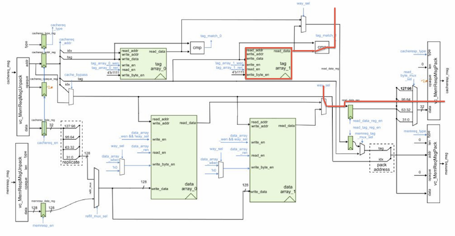
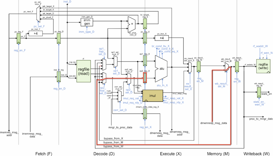
So from the end of the M stage of the LW instruction, to the end of the D stage of the ADDI instruction. Bypass paths are often on the critical path, and this specific path is always difficult to deal with. We could eliminate this critical path by removing the bypass path from M to D, but this would really only reduce the cycle time by 100-200ps. A more promising option would be to try and optimize the data cache design. We could try and optimize some of the logic on the critical path (e.g., the tag comparator or various muxes). We could also pipeline the data cache which would reduce the cycle time by increase the cache hit latency to two cycles.
We might also want to take a more detailed look at the power breakdown for the complete microbenchmark is shown below, but since this includes time spent in initialization and verification, we should be careful how we interpret these results.
                                               Int      Switch   Leak     Total
 Hierarchy                                     Power    Power    Power    Power    %
 ---------------------------------------------------------------------------------------
 ProcMemXcel_null_rtl                          5.22e-02 1.44e-02 2.39e-03 6.89e-02 100.0
   proc (ProcPRTL)                             1.17e-02 6.02e-03 6.89e-04 1.84e-02  26.7
    ctrl (ProcCtrlPRTL)                        1.02e-03 5.20e-04 3.74e-05 1.58e-03   2.3
    dpath (ProcDpathPRTL)                      9.56e-03 4.72e-03 5.90e-04 1.49e-02  21.6
      alu_X (AluPRTL)                          1.06e-03 9.82e-04 6.96e-05 2.11e-03   3.1
      imul (IntMulScycleRTL)                   2.38e-03 1.42e-03 1.43e-04 3.95e-03   5.7
      rf (RegisterFile)                        1.49e-03 3.98e-04 1.94e-04 2.08e-03   3.0
    imemreq_queue (TwoElementBypassQueue)      6.68e-04 1.43e-04 2.64e-05 8.37e-04   1.2
    xcelreq_queue (SingleElementBypassQueue)   6.85e-05 2.07e-05 8.67e-06 9.79e-05   0.1
  xcel (NullXcel)                              8.93e-05 3.48e-05 1.88e-05 1.43e-04   0.2
  imem (BlockingCachePRTL_0)                   2.76e-02 2.91e-03 7.65e-04 3.13e-02  45.4
    resp_bypass (SingleElementBypassQueue_0)   5.34e-04 1.79e-04 1.84e-05 7.31e-04   1.1
    ctrl (BlockingCacheCtrlPRTL_0)             2.46e-03 1.04e-03 3.13e-04 3.81e-03   5.5
    dpath (BlockingCacheDpathPRTL_0)           2.46e-02 1.63e-03 4.30e-04 2.66e-02  38.6
      tag_array_0 (SRAM_32x256_1P_wrapper_1)   2.41e-03 1.48e-05 4.77e-05 2.47e-03   3.6
      tag_array_1 (SRAM_32x256_1P_wrapper_0)   2.39e-03 1.10e-05 4.72e-05 2.45e-03   3.5
      data_array_0 (SRAM_128x256_1P_wrapper_0) 8.54e-03 4.16e-05 1.02e-04 8.69e-03  12.6
      data_array_1 (SRAM_128x256_1P_wrapper_1) 8.49e-03 5.50e-06 1.05e-04 8.60e-03  12.5
      read_data_reg (RegEnRst_1)               1.68e-03 7.85e-04 2.46e-05 2.49e-03   3.6
  funnel (Funnel)                              6.74e-05 4.88e-05 5.90e-06 1.22e-04   0.2
  router (Router)                              4.63e-05 4.49e-05 8.46e-06 9.96e-05   0.1
  dmem (BlockingCachePRTL_1)                   1.20e-02 3.92e-03 8.84e-04 1.68e-02  24.3
    resp_bypass (SingleElementBypassQueue_1)   1.27e-04 2.94e-05 2.39e-05 1.80e-04   0.3
    ctrl (BlockingCacheCtrlPRTL_1)             3.39e-03 2.67e-03 3.33e-04 6.40e-03   9.3
    dpath (BlockingCacheDpathPRTL_1)           7.97e-03 9.80e-04 5.20e-04 9.47e-03  13.7
      tag_array_0 (SRAM_32x256_1P_wrapper_3)   7.59e-04 2.17e-05 4.44e-05 8.25e-04   1.2
      tag_array_1 (SRAM_32x256_1P_wrapper_2)   5.29e-04 2.69e-06 4.44e-05 5.76e-04   0.8
      data_array_0 (SRAM_128x256_1P_wrapper_2) 3.06e-03 2.38e-05 1.02e-04 3.19e-03   4.6
      data_array_1 (SRAM_128x256_1P_wrapper_3) 2.10e-03 7.34e-07 1.02e-04 2.20e-03   3.2
      read_data_reg (RegEnRst_3)               3.44e-04 2.21e-04 3.39e-05 5.99e-04   0.9
At a high-level we can see that 45% of the power is spent in the instruction cache, 25% of the power is spent in the data cache, and 27% of the power is spent in the processor itself. Notice that more power is spent in the instruction cache since it is accessed almost every cycle, while the data cahce is only accessed on LW/SW instructions. Almost 70% of the power is spent in the memory system. This is not too surprising. SRAMs often consume a significant fraction of the power in many ASICs. Also note that the multiplier consumes ~6% of the power, but the multiplier is hardly used in this microbenchmark! This is a great example where we might want to use either data or clock gating to reduce the power consumption of an unused functional unit.
The area breakdown is shown below.
                          Global         Local
                          Cell Area      Cell Area
                          -------------- ------------------------
 Hierarchical cell        Abs                    Non     Black-
                          Total    %     Comb    Comb    boxes
 ------------------------ -------- ----- ------- ------- --------  --------------------------
 ProcMemXcel_null_rtl     893919.8 100.0  1781.4     0.0      0.0  ProcMemXcel_null_rtl
 proc                     126491.4  14.2   381.5     0.0      0.0  ProcPRTL
 proc/ctrl                  6028.1   0.7  3123.3  1232.1      0.0  ProcCtrlPRTL
 proc/dpath               111337.5  12.5   246.0     0.0      0.0  ProcDpathPRTL
 proc/dpath/alu_X          14574.1   1.6 14574.1     0.0      0.0  AluPRTL
 proc/dpath/imul           25702.5   2.9 21805.0     0.0      0.0  IntMulScycleRTL
 proc/dpath/rf             41919.8   4.7 16134.4 24684.1      0.0  RegisterFile
 xcel                       3446.7   0.4   251.5     0.0      0.0  NullXcel
 imem                     373501.9  41.8   371.4     0.0      0.0  BlockingCachePRTL_0
 imem/ctrl                 68185.4   7.6  1158.4    99.5      0.0  BlockingCacheCtrlPRTL_0
 imem/dpath               302905.5  33.9  4264.2     0.0      0.0  BlockingCacheDpathPRTL_0
 imem/dpath/tag_array_0    24259.1   2.7   141.9     0.0  24117.2  SRAM_32x256_1P_wrapper_1
 imem/dpath/tag_array_1    24242.5   2.7   125.3     0.0  24117.2  SRAM_32x256_1P_wrapper_0
 imem/dpath/data_array_0  118078.9  13.2   120.7     0.0 117958.2  SRAM_128x256_1P_wrapper_0
 imem/dpath/data_array_1  118400.6  13.2   442.3     0.0 117958.2  SRAM_128x256_1P_wrapper_1
 funnel                      863.5   0.1   768.6     0.0      0.0  Funnel
 router                      794.4   0.1   794.4     0.0      0.0  Router
 dmem                     387040.2  43.3   491.2     0.0      0.0  BlockingCachePRTL_1
 dmem/ctrl                 70902.3   7.9  1293.0    99.5      0.0  BlockingCacheCtrlPRTL_1
 dmem/dpath               313110.4  35.0  8994.8     0.0      0.0  BlockingCacheDpathPRTL_1
 dmem/dpath/tag_array_0    24174.3   2.7    57.1     0.0  24117.2  SRAM_32x256_1P_wrapper_3
 dmem/dpath/tag_array_1    24146.7   2.7    29.4     0.0  24117.2  SRAM_32x256_1P_wrapper_2
 dmem/dpath/data_array_0  118081.7  13.2   123.4     0.0 117958.2  SRAM_128x256_1P_wrapper_2
 dmem/dpath/data_array_1  118086.3  13.2   128.1     0.0 117958.2  SRAM_128x256_1P_wrapper_3
 ------------------------ -------- ----- ------- ------- --------  --------------------------
Notice that over 80% of the area is in the caches, and more specifically, approximately 60% of the area is in the generated SRAMs. This is not unusual. SRAMs often consume a significant fraction of the area in many ASICs.
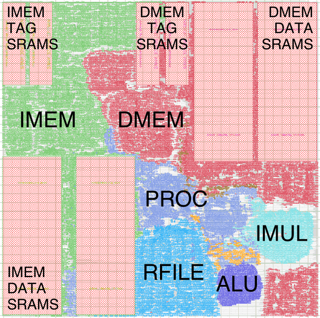
The following figure shows an amoeba plot of the baseline processor. The instruction cache is shown in green while the data memory is shown in red. The large rectangles correspond to the various SRAMs used in the caches. Since the caches are two-way set associative, there are two smaller SRAMs to store the tags and two larger SRAMs to store the data. The processor is shown in blue/purple. The register file, single-cycle multiplier, and integer ALU are also explicitly shown. Notice how the tools try to group cells from the same module together (e.g., the cells for the integer ALU are all clumped together), although sometimes the tools will spread a module apart (e.g., a portion of the data cache ends up in the lower-right corner).
VVADD Accelerator FL, CL, and RTL Models
We will take an incremental approach when designing, implementing, testing, and evaluating accelerators. We can use test sources, sinks, and memories to create a test harness that will enable us to explore the accelerator cycle-level performance and the ASIC area, energy, and timing in isolation. Only after we are sure that we have a reasonable design-point should we consider integrating the accelerator with the processor.
All accelerators have an xcel minion interface along with a standard mem master interface. The messages sent over the xcel minion interface allows the test harness or processor to read and write accelerator registers. These accelerator registers can be real registers that hold configuration information and/or results, or these accelerator registers can just be used to trigger certain actions. The messages sent over the xcel.req interface from the test harness or processor to the accelerator have the following format:
   1b     5b      32b
 +------+-------+-----------+
 | type | raddr | data      |
 +------+-------+-----------+
The 1-bit type field indicates if this messages if for reading (0) or
writing (1) an accelerator register, the 5-bit raddr field specifies
which accelerator register to read or write, and the 32-bit data field
is the data to be written. For every accelerator request, the accelerator
must send back a corresponding accelerator response over the xcel.resp
interface. These response messages have the following format:
   1b     32b
 +------+-----------+
 | type | data      |
 +------+-----------+
The 1-bit type field gain indicates if this response is from if for
reading (0) or writing (1) an accelerator register, and the 32-bit data
field is the data read from the corresponding accelerator register. Every
accelerator is free to design its own accelerator protocol by defining
the meaning of reading/writing the 32 accelerator registers.
We have implemented a null accelerator which we can use when we don’t
want to integrate a “real” accelerator, but this null accelerator is also
useful in illustrating the basic accelerator interface. The null
accelerator has a single accelerator register (xr0) which can be read and
written. Take a closer look at this null accelerator in
sim/proc/NullXcelRTL.py.
    @update
    def block():

      # Mux to force xcelresp data to zero on a write
      # Enable xr0 only upon write requests and both val/rdy on resp side

      if s.xcelreq_q.send.msg.type_ == XCEL_TYPE_WRITE:
        s.xr0.en @= s.xcel.resp.val & s.xcel.resp.rdy
        s.xcel.resp.msg.data @= 0
      else:
        s.xr0.en @= 0
        s.xcel.resp.msg.data @= s.xr0.out
The null accelerator simply waits for a xcel.req message to arrive. If
that message is a read, then it reads the xr0 register into the
xcelresp message. If that message is a write, then it sets the enable of
the xr0 register so that the new value is flopped in at the end of the
cycle. Here is a unit test which writes a value to the null accelerator’s
xr0 register and then reads it back:
 % cd $TOPDIR/sim/build
 % pytest ../proc/test/NullXcelRTL_test.py -k basic -s

  1r                >               |.           > .
  2r                >               |.           > .
  3:                >               |.           > .
  4:                >               |.           > .
  5:                >               |.           > .
  6:                >               |.           > .
  7: wr:00:0000000a > wr:00:0000000a|            >
  8: rd:00:         > rd:00:        |wr:         > wr:
  9:                >               |rd:0000000a > rd:0000000a
 10:                >               |.           > .
From the line trace, you can see the write request message (with write data 0x0a) going into the accelerator, and then the write response being returned on the next cycle. You can also see the read request message going into the accelerator, and then the read response being returned (with read data 0x0a) again on the next cycle.
The vvadd accelerator is obviously more sophisticated. Accelerator
protocols are usually defined as a comment at the top of the FL model, so
take a closer look at the vvadd accelerator FL model in
sim/tut9_xcel/VvaddXcelFL.py. The vvadd accelerator protocol defines
the accelerator registers as follows:
- xr0 : go/done
- xr1 : base address of the array src0
- xr2 : base address of the array src1
- xr3 : base address of the array dest
- xr4 : size of the array
The actual protocol involves the following steps:
- Write the base address of src0 to xr1
- Write the base address of src1 to xr2
- Write the base address of dest to xr3
- Write the number of elements in the array to xr4
- Tell accelerator to go by writing xr0
- Wait for accelerator to finish by reading xr0, result will be 1
A close look at the vvadd accelerator FL model shows that most of the work is really in managing this accelerator protocol. The accelerator waits for accelerator requests, updates its internal state registers, and when it receives a write to xr0 it starts doing the actual vvadd computation. The FL model makes use of method-based interfaces to simplify interacting with the memory system. Let’s run the unit tests on the FL model first:
 % cd $TOPDIR/sim/build
 % pytest ../tut9_xcel/test/VvaddXcelFL_test.py -v
The vvadd accelerator CL model is actually very close to the RTL
implementation largely due to the need to carefully interact with the
latency insensitive memory interface. CL modeling may or may not be
useful in this context. The vvadd accelerator RTL model is in
sim/tut9_xcel/VvaddXcelPRTL.py and (roughly) implements the following
FSM:
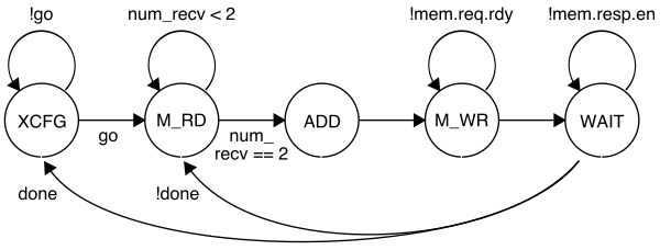
While the accelerator is in the XCFG state, it will update its internal registers when it receives accelerator requests. When the accelerator receives a write to xr0 it moves into the M_RD state. While in the M_RD state, the accelerator will send out two memory read requests to read the current element from each source array. In the ADD state, the accelerator will do the actual addition, and in the M_WR state, the accelerator will send out the memory write request to write the result to the destination array. The accelerator will wait in the final WAIT state until it receives the memory write response, and then will either move back into the M_RD state if there is another element to be processed, or move into the XCFG state if we have processed all elements in the array.
The accelerator is not implemented with a control/datapath split because the accelerator is almost entirely control logic; it was just simpler to implement the accelerator as a single model. When a model is almost all control logic or almost all datapath logic, then a control/datapath split may be more trouble than its worth.
Let’s run the unit tests for all of the vvadd accelerator models:
 % cd $TOPDIR/sim/build
 % pytest ../tut9_xcel
 % pytest ../tut9_xcel --test-verilog
We have also included a simulator for just the vvadd accelerator in isolation which can be used to evaluate its performance.
 % cd $TOPDIR/sim/build
 % ../tut9_xcel/vvadd-xcel-sim --impl rtl --input multiple --stats
 num_cycles = 1058
We could use the simulator to help evaluate the cycle-level performance of the accelerator on various different datasets as we try out various optimizations.
VVADD Accelerator ASIC
We can now push the vvadd accelerator through the ASIC flow in isolation to get a feel for the area, timing, and energy. We first need to run all of the tests to generate appropriate Verilog test benches for 4-state and gate-level simulation. We can then use the evaluation simulator to translate the accelerator into Verilog and to generate the VCD file we need for energy analysis.
 % cd $TOPDIR/sim/build
 % pytest ../tut9_xcel --test-verilog --dump-vtb
 % ../tut9_xcel/vvadd-xcel-sim --impl rtl --input multiple \
     --stats --translate --dump-vtb
 ...
 VvaddXcelRTL__pickled.v
 VvaddXcelRTL_vvadd-xcel-rtl-multiple_tb.v
We will use a rather conservative clock constraint of 3.0ns since that is what we are hoping to hit for the baseline processor. Our goal in designing these accelerators is just to ensure the accelerator doesn’t increase the critical path of the processor; there is no benefit in pushing the accelerator to have a cycle time which is less than the processor since this will not help the overall cycle time of the processor, memory, accelerator composition. We can now push the accelerator through the flow.
 % mdkir -p $TOPDIR/asic/build-vvadd-xcel
 % cd $TOPDIR/asic/build-vvadd-xcel
 % mflowgen run --design ../tut9-vvadd-xcel
 % make
The accelerator has no trouble meeting timing. If the accelerator did have trouble meeting the 3.0ns clock constraint, then we could do timing optimizations on the accelerator in isolation before moving onto the processor, memory, accelerator composition. We can also do area and energy optimization on the accelerator in isolation.
Integrating the TinyRV2 Processor and the VVADD Accelerator
Now that we have unit tested and evaluated both the baseline TinyRV2 pipelined processor and the vvadd accelerator in isolation, we are finally ready to compose them. The processor will send messages to the accelerator by reading and writing 32 special CSRs using the standard CSRW and CSRR instructions. These 32 special CSRs are as follows:
  0x7e0 : accelerator register  0 (xr0)
  0x7e1 : accelerator register  1 (xr1)
  0x7e2 : accelerator register  2 (xr2)
  ...
  0x7ff : accelerator register 31 (xr31)
When the processor uses a CSRW instruction to write an accelerator register, it first reads the general-purpose register file to get the source value, creates a new accelerator request message, then sends this message to the accelerator through the xcel.req interface in the X stage. The processor waits for the response message to be returned through the xcel.resp interface in the M stage. The processor uses a CSRR instruction to read an accelerator register in a similar way, except that when the response message is returned in the M stage, the data from the accelerator is sent down the pipeline and written into the general-purpose register file in the W stage.
Here is a simple assembly sequence which will write the value 1 to the
null accelerator’s only accelerator register, read that value back from
the accelerator register, and write the value to general-purpose register
x2.
  addi x1, x0, 1
  csrw 0x7e0, x1
  csrr x2, 0x7e0
You can run a simple test of using the CSRW/CSRR instructions to write/read an accelerator register like this:
 % cd $TOPDIR/sim/build
 % pytest ../proc/test/ProcFL_xcel_test.py
 % pytest ../proc/test/ProcRTL_xcel_test.py
 % pytest ../proc/test/ProcRTL_xcel_test.py -k [bypass -s

     src        F-stage  D-stage         X     M     W     xcelreq         xcelresp    sink
 -----------------------------------------------------------------------------------------------
  2r .        >         |               |     |     |     |              |.          > .
  3: .        >         |               |     |     |     |              |.          > .
  4: .        > 00000200|               |     |     |     |              |.          > .
  5: .        > #       |#              |     |     |     |              |.          > .
  6: .        > #       |#              |     |     |     |              |.          > .
  7: deadbeef > 00000204|csrr x02, 0xfc0|     |     |     |              |.          >
  8: #        > 00000208|nop            |csrr |     |     |              |.          >
  9: #        > 0000020c|nop            |nop  |csrr |     |              |.          >
 10: #        > 00000210|nop            |nop  |nop  |csrr |              |.          >
 11: #        > 00000214|csrw 0x7e0, x02|nop  |nop  |nop  |              |.          >
 12: #        > 00000218|csrr x03, 0x7e0|csrw |nop  |nop  |wr:00:deadbeef|.          >
 13: #        > 0000021c|nop            |csrrx|csrw |nop  |rd:00:        |wr:        >
 14: #        > 00000220|nop            |nop  |csrrx|csrw |              |rd:deadbeef>
 15: #        > 00000224|nop            |nop  |nop  |csrrx|              |.          >
 16: #        > 00000228|csrw 0x7c0, x03|nop  |nop  |nop  |              |.          >
 17: deadbe00 > 0000022c|csrr x02, 0xfc0|csrw |nop  |nop  |              |.          >
 18: #        > 00000230|nop            |csrr |csrw |nop  |              |.          >
 19: #        > 00000234|nop            |nop  |csrr |csrw |              |.          > deadbeef
 20: #        > 00000238|csrw 0x7e0, x02|nop  |nop  |csrr |              |.          >
 21: #        > 0000023c|csrr x03, 0x7e0|csrw |nop  |nop  |wr:00:deadbe00|.          >
 22: #        > 00000240|nop            |csrrx|csrw |nop  |rd:00:        |wr:        >
 23: #        > 00000244|nop            |nop  |csrrx|csrw |              |rd:deadbe00>
 24: #        > 00000248|csrw 0x7c0, x03|nop  |nop  |csrrx|              |.          >
 25: 00adbe00 > 0000024c|csrr x02, 0xfc0|csrw |nop  |nop  |              |.          >
 26: #        > 00000250|nop            |csrr |csrw |nop  |              |.          >
 27: #        > 00000254|csrw 0x7e0, x02|nop  |csrr |csrw |              |.          > deadbe00
 28: #        > 00000258|csrr x03, 0x7e0|csrw |nop  |csrr |wr:00:00adbe00|.          >
 29: #        > 0000025c|nop            |csrrx|csrw |nop  |rd:00:        |wr:        >
 30: #        > 00000260|csrw 0x7c0, x03|nop  |csrrx|csrw |              |rd:00adbe00>
 31: dea00eef > 00000264|csrr x02, 0xfc0|csrw |nop  |csrrx|              |.          >
 32: .        > 00000268|csrw 0x7e0, x02|csrr |csrw |nop  |              |.          >
 33: .        > 0000026c|csrr x03, 0x7e0|csrw |csrr |csrw |wr:00:dea00eef|.          > 00adbe00
 34: .        > #       |#              |csrrx|csrw |csrr |rd:00:        |wr:        >
 35: .        > 00000270|csrw 0x7c0, x03|     |csrrx|csrw |              |rd:dea00eef>
 36: .        > 00000274|               |csrw |     |csrrx|              |.          >
 37: .        > 00000278|               |???? |csrw |     |              |.          >
 38: .        > 0000027c|               |???? |???? |csrw |              |.          > dea00eef
 39: .        > 00000280|               |???? |???? |???? |              |.          > .
I have cleaned up the line trace a bit to annotate the columns and make it more compact. You can see the processor executing CSRW/CSRR instructions to 0x7e0 which is accelerator register 0. This results in the processor sending accelerator requests to the null accelerator, and then the accelerator sending the corresponding accelerator responses back to the processor.
Also notice the need for the processor to add new RAW dependency stall logic. CSRR instructions which read from accelerator registers send out the xcel.req in the X stage and receive the xcelresp in the M stage. This means we cannot bypass data from a CSRR instruction if it is in the X stage since the data has not returned from the accelerator yet. In cycle 34, the CSRW instruction in the decode stage needs to stall to wait for the CSRR instruction in the X stage to move into the M stage.
Accelerating a TinyRV2 Microbenchmark
To use an accelerator from a C microbenchmark, we can use the same GCC
inline assembly extensions we used to write the stats_en CSR earlier in
the tutorial. Take a closer look at the app/ubmark/ubmark-null-xcel.c
example:
 __attribute__ ((noinline))
 unsigned int null_xcel( unsigned int in )
 {
   unsigned int result;
   asm volatile (
     "csrw 0x7E0,     %[in];\n"
     "csrr %[result], 0x7E0;\n"

     // Outputs from the inline assembly block

     : [result] "=r"(result)

     // Inputs to the inline assembly block

     : [in] "r"(in)

   );
   return result;
 }
We are inserting a CSRW instruction to copy the value passed to this
function through the in argument, and then we are using an CSRR
instruction to retrieve the same value from the null accelerator. Notice
that unlike the inline assembly we used when setting the stats_en CSR,
here we also need to handle outputs from the assembly block. Again, you
can find out more about inline assembly syntax here:
Let’s cross-compile this example. Note that you cannot natively compile a microbenchmark that makes use of an accelerator, since x86 does not have any accelerators!
 % cd $TOPDIR/app/build
 % make ubmark-null-xcel
 % riscv32-objdump ubmark-null-xcel | less
 000002c0 <null_xcel(unsigned int)>:
    2c0:  csrw 0x7e0, x10
    2c4:  csrr x10, 0x7e0
    2c8:  jalr x0,  x1, 0
Always a good idea to use riscv32-objdump so you can verify your C code
is compiling as expected. Here we can see that the null_xcel function
compiles into a CSRW, CSRR, and JALR instruction as expected. We should
now run this microbenchmark on our ISA simulator to verify it works, and
then we can run it on our RTL simulator.
 % cd $TOPDIR/sim/build
 % ../pmx/pmx-sim ../../app/build/ubmark-null-xcel
 % ../pmx/pmx-sim --proc-impl rtl --cache-impl rtl --xcel-impl null-rtl \
     --trace ../../app/build/ubmark-null-xcel
Let’s turn out attention to our vvadd accelerator. Take a closer look at
the accelerated version of the vvadd microbenchmark in
app/ubmark/ubmark-vvadd-xcel.c:
 __attribute__ ((noinline))
 void vvadd_xcel( int *dest, int *src0, int *src1, int size )
 {
   asm volatile (
     "csrw 0x7E1, %[src0];\n"
     "csrw 0x7E2, %[src1];\n"
     "csrw 0x7E3, %[dest];\n"
     "csrw 0x7E4, %[size];\n"
     "csrw 0x7E0, x0     ;\n"
     "csrr x0,    0x7E0  ;\n"

     // Outputs from the inline assembly block

     :

     // Inputs to the inline assembly block

     : [src0] "r"(src0),
       [src1] "r"(src1),
       [dest] "r"(dest),
       [size] "r"(size)

     // Tell the compiler this accelerator read/writes memory

     : "memory"
   );
 }
Notice that our use of the CSRW/CSRR instructions corresponds exactly to
the accelerator protocol described above. We first write the source base
pointers, the destination base pointer, and the size before starting the
accelerator by writing to xr0 and then waiting for the accelerator to
finish by reading xr0. We need a final "memory" argument in our
inline assembly block to tell the compiler that this accelerator reads
and writes memory. Let’s cross-compile the accelerated version of the
vvadd with a similar test as we used earlier in this tutorial.
 % cd $TOPDIR/app/build
 % make ubmark-vvadd-xcel-test1
 % riscv32-objdump ubmark-vvadd-xcel-test1 | less
 0000060 <vvadd_xcel(int*, int*, int*, int)>:
    604:  csrw 0x7e1, x11
    608:  csrw 0x7e2, x12
    60c:  csrw 0x7e3, x10
    610:  csrw 0x7e4, x13
    614:  csrw 0x7e0, x0
    618:  csrr x0, 0x7e0
    61c:  jalr x0, x1, 0
Everything looks as expected, so we can now test our accelerated vvadd on the ISA simulator.
 % cd $TOPDIR/sim/build
 % ../pmx/pmx-sim --xcel-impl vvadd-fl ../../app/build/ubmark-vvadd-xcel-test1
Notice that we needed to specify the accelerator implementation as a command line option. If we forgot to include this option, then the simulator would use the null accelerator and clearly the accelerated vvadd microbenchmark does not work with the null accelerator! Finally, we can run the same test on the RTL implementation of the processor augmented with the RTL implementation of the vvadd accelerator:
 % cd $TOPDIR/sim/build
 % ../pmx/pmx-sim --proc-impl rtl --cache-impl rtl --xcel-impl vvadd-rtl \
     ../../app/build/ubmark-vvadd-xcel-test1
Now that we know that our accelerated implementation of vvadd is passing our tests, we can evaluate its performance using an evaluation program which serves as the actual microbenchmark just like with our pure-software implementation. We build it, make sure it works on the ISA simulator, and then evaluate its performance on the RTL implementation of the processor augmented with the RTL implementation of the vvadd accelerator:
 % cd $TOPDIR/app/build
 % make ubmark-vvadd-xcel-eval

 % cd $TOPDIR/sim/build
 % ../pmx/pmx-sim --xcel-impl vvadd-fl ../../app/build/ubmark-vvadd-xcel-eval
 % ../pmx/pmx-sim --proc-impl rtl --cache-impl rtl --xcel-impl vvadd-rtl \
    --stats ../../app/build/ubmark-vvadd-xcel-eval
 num_cycles =  1109
 num_insts_on_processor =  14
Recall that the pure-software vvadd microbenchmark required 1318 cycles. So our accelerator results in a cycle-level speedup of 1.19x. We might ask, where did this speedup come from? Why isn’t the speedup larger? Let’s look at the line trace.
 % cd $TOPDIR/sim/build
 % ../pmx/pmx-sim --proc-impl rtl --cache-impl rtl --xcel-impl vvadd-rtl \
     --trace ../../app/build/ubmark-vvadd-xcel-eval > ubmark-vvadd-xcel.trace
Here is what the line trace looks like for the initial configuration of the accelerator and the first two iterations of the vvadd loop:
cyc   F-stage  D-stage              X     M     W      I$   D$  xcelreq        ST              xcel->memreq            xcel<-memresp    xcelresp
------------------------------------------------------------------------------------------------------------------------------------------------
818:  00000308|csrw 0x7c1, x15     |addi |bne  |addi [(TC)|(I )]              (X  0:0:00000000|.                                       ).
819:  0000030c|addi x18, x00, 0x400|csrw |addi |bne  [(TC)|(I )]              (X  0:0:00000000|.                                       ).
820:  #       |addi x11, x18, 0x190|addi |csrw |addi [(TC)|(I )]              (X  0:0:00000000|.                                       ).
821:  #       |                    |addi |addi |csrw [(RR)|(I )]              (X  0:0:00000000|.                                       ).
822: -#       |                    |     |addi |addi [(RW)|(I )]              (X  0:0:00000000|.                                       ).
823: -#       |                    |     |     |addi [(RU)|(I )]              (X  0:0:00000000|.                                       ).
824: -#       |                    |     |     |     [(RD)|(I )]              (X  0:0:00000000|.                                       ).
825: -00000310|                    |     |     |     [(Wm)|(I )]              (X  0:0:00000000|.                                       ).
826: -#       |addi x12, x00, 0x400|     |     |     [(I )|(I )]              (X  0:0:00000000|.                                       ).
827: -00000314|                    |addi |     |     [(TC)|(I )]              (X  0:0:00000000|.                                       ).
828: -00000318|addi x10, x09, 0x000|     |addi |     [(TC)|(I )]              (X  0:0:00000000|.                                       ).
829: -~       |jal  x01, 0x1fff30  |addi |     |addi [(TC)|(I )]              (X  0:0:00000000|.                                       ).
830: -00000248|                    |jal  |addi |     [(TC)|(I )]              (X  0:0:00000000|.                                       ).
831: -0000024c|csrw 0x7e1, x11     |     |jal  |addi [(TC)|(I )]              (X  0:0:00000000|.                                       ).
832: -#       |csrw 0x7e2, x12     |csrw |     |jal  [(TC)|(I )]wr:01:00000590(X  0:0:00000000|.                                       ).
833: -#       |                    |csrw |csrw |     [(RR)|(I )]wr:02:00000400(X  0:0:00000000|.                                       )wr:
834: -#       |                    |     |csrw |csrw [(RW)|(I )]              (X  0:0:00000000|.                                       )wr:
835: -#       |                    |     |     |csrw [(RU)|(I )]              (X  0:0:00000000|.                                       ).
836: -#       |                    |     |     |     [(RD)|(I )]              (X  0:0:00000000|.                                       ).
837: -00000250|                    |     |     |     [(Wm)|(I )]              (X  0:0:00000000|.                                       ).
838: -#       |csrw 0x7e3, x10     |     |     |     [(I )|(I )]              (X  0:0:00000000|.                                       ).
839: -00000254|                    |csrw |     |     [(TC)|(I )]wr:03:000ffe3c(X  0:0:00000000|.                                       ).
840: -00000258|csrw 0x7e4, x13     |     |csrw |     [(TC)|(I )]              (X  0:0:00000000|.                                       )wr:
841: -0000025c|csrw 0x7e0, x00     |csrw |     |csrw [(TC)|(I )]wr:04:00000064(X  0:0:00000000|.                                       ).
842: -#       |csrr x00, 0x7e0     |csrw |csrw |     [(TC)|(I )]wr:00:00000000(X  0:0:00000000|.                                       )wr:
843: -#       |                    |csrrx|csrw |csrw [(RR)|(I )]rd:00:        (X  0:0:00000000|.                                       )wr:
844: -#       |                    |     |#    |csrw [(RW)|(I )].             (RD 0:0:00000000|rd:00:00000590:                         ).
845: -#       |                    |     |#    |     [(RU)|(TC)].             (RD 0:0:00000000|#                                       ).
846: -#       |                    |     |#    |     [(RD)|(RR)].             (RD 0:0:00000000|#                                       ).
847: -#       |                    |     |#    |     [(Wm)|(RW)].             (RD 0:0:00000000|#                                       ).
848: -#       |                    |     |#    |     [(Wm)|(RU)].             (RD 0:0:00000000|#                                       ).
849: -#       |                    |     |#    |     [(Wm)|(RD)].             (RD 0:0:00000000|#                                       ).
850: -#       |                    |     |#    |     [(Wm)|(Wm)].             (RD 0:0:00000000|#                       rd:01:0:00000017).
851: -#       |                    |     |#    |     [(Wm)|(I )].             (RD 1:1:00000000|rd:00:00000400:                         ).
852: -#       |                    |     |#    |     [(Wm)|(TC)].             (RD 0:1:00000000|.                                       ).
853: -#       |                    |     |#    |     [(Wm)|(RR)].             (RD 0:1:00000000|.                                       ).
854: -#       |                    |     |#    |     [(Wm)|(RW)].             (RD 0:1:00000000|.                                       ).
855: -#       |                    |     |#    |     [(Wm)|(RU)].             (RD 0:1:00000000|.                                       ).
856: -#       |                    |     |#    |     [(Wm)|(RD)].             (RD 0:1:00000000|.                                       ).
857: -#       |                    |     |#    |     [(Wm)|(Wm)].             (RD 0:1:00000000|.                       rd:01:0:00000033).
858: -#       |                    |     |#    |     [(Wm)|(I )].             (RD 1:2:00000000|.                                       ).
859: -#       |                    |     |#    |     [(Wm)|(I )].             (+  0:2:00000033|.                                       ).
860: -#       |                    |     |#    |     [(Wm)|(I )].             (WR 0:2:00000033|wr:00:000ffe3c:0000004a                 ).
861: -#       |                    |     |#    |     [(Wm)|(TC)].             (W  0:0:00000033|.                       wr:01:1:        ).
862: -#       |                    |     |#    |     [(Wm)|(WD)].             (W  1:0:00000000|.                                       ).
863: -#       |                    |     |#    |     [(Wm)|(I )].             (RD 0:0:00000000|rd:00:00000594:                         ).
864: -#       |                    |     |#    |     [(Wm)|(TC)].             (RD 0:0:00000000|rd:00:00000404:         rd:01:1:00000000).
865: -#       |                    |     |#    |     [(Wm)|(TC)].             (RD 1:1:00000000|.                       rd:01:1:00000047).
866: -#       |                    |     |#    |     [(Wm)|(I )].             (RD 1:2:00000000|.                                       ).
867: -#       |                    |     |#    |     [(Wm)|(I )].             (+  0:2:00000047|.                                       ).
868: -#       |                    |     |#    |     [(Wm)|(I )].             (WR 0:2:00000047|wr:00:000ffe40:00000047                 ).
869: -#       |                    |     |#    |     [(Wm)|(TC)].             (W  0:0:00000047|.                       wr:01:1:        ).
870: -#       |                    |     |#    |     [(Wm)|(WD)].             (W  1:0:00000000|.                                       ).
I have cleaned up the line trace a bit to annotate the columns and make
it more compact. The ST column is the current state of the vvadd
accelerator FSM. You can see the processor executing the CSRW
instructions to configure the accelerator, and these instructions then
turn into messages over the xcel.req interface. The accelerator is in the
XCFG state receiving these messages until it receives the write to xr0
which causes the accelerator to move into the RD stage. The accelerator
sends the first memory read request request into the memory system, but
this causes a data cache miss so the accelerator stalls in the RD state.
Once the data from the first read is returned, the accelerator sends out
a second memory read request but again this causes a cache miss. Once the
data from both reads have returned, the accelerator does the addition,
and finally sends a memory write request with the result into the memory
system. The second iteration is faster for the same reason the second
iteration of the pure-software vvadd microbenchmark was faster: we are
exploiting spatial locality in the data cache so the sequential reads hit
in the same cache line.
We know that every fourth iteration should look like the first iteration
(19 cycles) and the remaining iterations should look like the second
iteration (8 cycles). Since there are 100 iterations, this means the
total number of cycles should be about 1075 cycles, but our simulator
reported 1109 cycles. Again, the discrepancy is due to the extra cycles
required to call and return from the vvadd_scalar function. So the
accelerator is a little faster than the processor since it requires fewer
cycles per iteration, but notice that the execution time is largely
dominated by the miss penalty. The accelerator does not really help
reduce nor hide this miss latency.
There is certainly room for improvement. We can probably remove some of the bubbles and improve the accelerator performance by a couple more cycles. The accelerator could also potentially use wide accesses to the data cache to retrieve four words at a time and then process all four words in parallel. The accelerator could also potentially achieve better performance by issuing multiple memory requests to a non-blocking cache. Eventually we should be able to optimize such an accelerator so that it is memory bandwidth limited (i.e., we are doing a memory request every cycle).
As with the pure-software vvadd microbenchmark, sometimes it is useful to run experiments where we assume a perfect cache to help isolate the impact of the memory system. Again, this is easy to do with our simulator. We simply avoid inserting any cache at all and instead have the processor directly communicate with the test memory. This means all memory requests take a single cycle.
 % cd $TOPDIR/sim/build
 % ../pmx/pmx-sim --proc-impl rtl --xcel-impl vvadd-rtl \
     --stats ../../app/build/ubmark-vvadd-xcel-eval
 num_cycles =  817
Recall the pure-software vvadd microbenchmark took 1012 cycles without any cache misses, so the accelerator is now able to improve the performance by 1.23x.
TinyRV2 Processor + VVADD Accelerator ASIC
NOTE: The cache is not quite ready to be pushed through the flow, so
for now the tutorial will just focus on pushing the processor through the
flow without the cache. Eventually, you would relace --cache-impl null
with --cache-impl rtl below to push the processor and cache through the
flow. Everywhere we see ProcXcel would be ProcMemXcel. We will also
include some results from previously pushing the processor, cache, and
accelerator through the flow.
Now that we have some results suggesting our vvadd accelerator is able to
improve the cycle-level performance by 1.19x, we can push the processor,
memory, accelerator composition through the flow to see the overall
impact on area, energy, and timing. We can use the pmx-sim simulator to
translate the processor and to generate a Verilog test benches that we
can also use for 4-state and gate-level simulation.
 % cd $TOPDIR/sim/build
 % ../pmx/pmx-sim --proc-impl rtl --cache-impl null --xcel-impl vvadd-rtl \
     --translate --dump-vtb ../../app/build/ubmark-vvadd-xcel-test1
 % ../pmx/pmx-sim --proc-impl rtl --cache-impl null --xcel-impl vvadd-rtl \
     --stats --translate --dump-vtb ../../app/build/ubmark-vvadd-xcel-eval
 % ls
 ...
 ProcMemXcel_vvadd__pickled.v
 ProcMemXcel_vvadd_rtl_pmx-sim-vvadd-rtl-ubmark-vvadd-xcel-test1_tb.v.cases
 ProcMemXcel_vvadd_rtl_pmx-sim-vvadd-rtl-ubmark-vvadd-xcel-eval_tb.v.cases
Then we create a build directory for the ASIC toolflow.
 % mkdir -p $TOPDIR/asic/build-tut9-pmx-vvadd
 % cd $TOPDIR/asic/build-tut9-pmx-vvadd
 % mflowgen run --design ../tut9-pmx-vvadd
Now we can push the design through the flow step-by-step:
 % cd $TOPDIR/asic/build-tut9-pmx-null
 % make brg-rtl-4-state-vcssim
 % make brg-synopsys-dc-synthesis
 % make post-synth-gate-level-simulation
 % make post-synth-power-analysis
 % make brg-cadence-innovus-signoff
 % make brg-flow-summary
Here is the summary:
==========================================================================
  Summary
==========================================================================

design_name = ProcXcel_vvadd_rtl

area & timing
  design_area   = 20059.858 um^2
  stdcells_area = 20059.858 um^2
  macros_area   = 0.0 um^2
  chip_area     = 59958.688 um^2
  core_area     = 28870.842 um^2
  constraint    = 3.0 ns
  slack         = 0.376 ns
  actual_clk    = 2.624 ns

==========================================================================
 4-State Sim Results
==========================================================================
[PASSED]: pmx-sim-vvadd-rtl-ubmark-vvadd-xcel-test1
[PASSED]: pmx-sim-vvadd-rtl-ubmark-vvadd-xcel-eval

==========================================================================
 Fast-Functional Sim Results
==========================================================================
[PASSED]: pmx-sim-vvadd-rtl-ubmark-vvadd-xcel-test1
[PASSED]: pmx-sim-vvadd-rtl-ubmark-vvadd-xcel-eval

==========================================================================
 Fast-Functional Power Analysis
==========================================================================

 power & energy

  pmx-sim-vvadd-rtl-ubmark-vvadd-xcel-test1.vcd
      exec_time = 652 cycles
      power     = 3.809 mW
      energy    = 7.4504 nJ

  pmx-sim-vvadd-rtl-ubmark-vvadd-xcel-eval.vcd
      exec_time = 2697 cycles
      power     = 3.79 mW
      energy    = 30.6649 nJ
You can run all the steps at once by just using the default make target
(i.e., just enter make). Our processor and accelerator passes 4-state
and gate-level simulation and meets timing. Note that as before you
cannot use the value for exec_time from this final summary. The
summary is reporting 2697 cycles because that includes the time for
initialization and verification, while the cycle count from pmx-sim
(i.e., 817) is only when stats are enabled.
We know from our earlier experiment with the dummy ubmark, that ~25.5nJ is spent on initialization and verification, so we can estimate the energy for just the vvadd accelerator to be 30.6-25.5 = 4.9nJ. Recall tha the energy for the pure-software implementation was 10.9nJ. This means the accelerator reduces the overall total energy by 10.9/4.9 = 2.2x!
NOTE: The rest of this section in the tutorial provides some results from a previous version which includes the cache. It is included here to give students some insight about a more realistic design that includes the processor and cache together pushed through the ASIC flow.
Notice that the area of the vvadd accelerator is 988,840 um^2, while the area of the baseline processor is 964,955 um^2. Adding the vvadd accelerator to the baseline processor results in an area overhead of just 2%, mostly due to the area consumed by the various queues in the design. The area breakdown confirms that most of the area stays the same except for the accelerator.
                          Global         Local
                          Cell Area      Cell Area
                          -------------- ------------------------
 Hierarchical cell        Abs                    Non     Black-
                          Total    %     Comb    Comb    boxes
 ------------------------ -------- ----- ------- ------- --------  --------------------------
 ProcMemXcel_vvadd_rtl    914452.1 100.0  1264.4     0.0      0.0  ProcMemXcel_vvadd_rtl
 proc                     124253.7  13.6   166.8     0.0      0.0  ProcPRTL
 proc/ctrl                  5759.0   0.6  2955.5  1219.2      0.0  ProcCtrlPRTL
 proc/dpath               108875.0  11.9   359.4     0.0      0.0  ProcDpathPRTL
 proc/dpath/alu_X          13868.2   1.5 13868.2     0.0      0.0  AluPRTL
 proc/dpath/imul           25097.0   2.7 21593.0     0.0      0.0  IntMulScycleRTL
 proc/dpath/rf             41881.1   4.6 16082.8 24684.1      0.0  RegisterFile
 xcel                      24461.1   2.7  6559.9  7196.7      0.0  VvaddXcelPRTL
 imem                     372201.5  40.7   182.4     0.0      0.0  BlockingCachePRTL_0
 imem/ctrl                 67863.8   7.4  1500.3    99.5      0.0  BlockingCacheCtrlPRTL_0
 imem/dpath               302570.9  33.1  4712.1     0.0      0.0  BlockingCacheDpathPRTL_0
 imem/dpath/tag_array_0    24130.1   2.6    12.9     0.0  24117.2  SRAM_32x256_1P_wrapper_1
 imem/dpath/tag_array_1    24130.1   2.6    12.9     0.0  24117.2  SRAM_32x256_1P_wrapper_0
 imem/dpath/data_array_0  117996.9  12.9    38.7     0.0 117958.2  SRAM_128x256_1P_wrapper_0
 imem/dpath/data_array_1  118013.5  12.9    55.2     0.0 117958.2  SRAM_128x256_1P_wrapper_1
 funnel                     1434.9   0.2  1166.7     0.0      0.0  Funnel
 router                     1217.4   0.1  1217.4     0.0      0.0  Router
 dmem                     389618.8  42.6   435.9     0.0      0.0  BlockingCachePRTL_1
 dmem/ctrl                 70591.7   7.7  1550.1    99.5      0.0  BlockingCacheCtrlPRTL_1
 dmem/dpath               315555.4  34.5  8992.9     0.0      0.0  BlockingCacheDpathPRTL_1
 dmem/dpath/tag_array_0    24138.4   2.6    21.1     0.0  24117.2  SRAM_32x256_1P_wrapper_3
 dmem/dpath/tag_array_1    24135.6   2.6    18.4     0.0  24117.2  SRAM_32x256_1P_wrapper_2
 dmem/dpath/data_array_0  118225.5  12.9   267.2     0.0 117958.2  SRAM_128x256_1P_wrapper_2
 dmem/dpath/data_array_1  118286.3  12.9   328.0     0.0 117958.2  SRAM_128x256_1P_wrapper_3
 ------------------------ -------- ----- ------- ------- --------  --------------------------
A close look at the critical path shows it to be similar to what we saw in the baseline processor, so the accelerator does not impact the overall cycle time.
We can use our earlier results for the energy overhead of initialization and verification to estimate the energy of using the vvadd accelerator to be 426-354 = 72nJ. This is about 50% of the energy required when using the pure-software vvadd microbenchmark. We can dig into the power reports, although this is somewhat complicated by the fact that the power reports are for the entire program execution as opposed to only when stats are enabled.
                                               Int      Switch   Leak     Total
Hierarchy                                      Power    Power    Power    Power    %
----------------------------------------------------------------------------------------
ProcMemXcel_vvadd_rtl                          4.53e-02 1.30e-02 2.51e-03 6.08e-02 100.0
  proc (ProcPRTL)                              9.74e-03 4.34e-03 6.67e-04 1.48e-02  24.3
    ctrl (ProcCtrlPRTL)                        6.96e-04 3.50e-04 3.22e-05 1.08e-03   1.8
    dpath (ProcDpathPRTL)                      8.21e-03 3.80e-03 5.65e-04 1.26e-02  20.7
      imul (IntMulScycleRTL)                   1.88e-03 1.08e-03 1.36e-04 3.10e-03   5.1
      alu_X (AluPRTL)                          8.59e-04 6.99e-04 6.01e-05 1.62e-03   2.7
      rf (RegisterFile)                        1.13e-03 2.86e-04 1.93e-04 1.61e-03   2.6
    imemreq_queue (TwoElementBypassQueue)      4.91e-04 1.00e-04 3.66e-05 6.27e-04   1.0
    xcelreq_queue (SingleElementBypassQueue)   6.99e-05 1.69e-05 8.22e-06 9.50e-05   0.2
  xcel (VvaddXcelPRTL)                         3.13e-03 1.08e-04 1.14e-04 3.36e-03   5.5
    idx (Reg_1)                                3.60e-04 7.73e-07 3.62e-06 3.65e-04   0.6
    base_dest (Reg_2)                          3.89e-04 5.60e-09 3.69e-06 3.93e-04   0.6
    sum_val (Reg_3)                            3.12e-04 2.94e-07 3.57e-06 3.15e-04   0.5
    base_src0 (Reg_0)                          3.32e-04 9.88e-10 3.43e-06 3.35e-04   0.6
    base_src1 (Reg_4)                          3.14e-04 2.59e-10 3.35e-06 3.18e-04   0.5
    size (Reg_5)                               3.59e-04 3.22e-09 3.62e-06 3.63e-04   0.6
    num_src0 (Reg_6)                           3.17e-04 7.83e-07 3.60e-06 3.21e-04   0.5
    num_src1 (Reg_7)                           3.15e-04 8.08e-07 3.59e-06 3.19e-04   0.5
    memreq_sent (Reg_1)                        4.53e-05 7.08e-07 4.63e-07 4.65e-05   0.1
    memrsp_recv (Reg_0)                        4.38e-05 4.96e-07 4.57e-07 4.48e-05   0.1
    xcelreq_q (SingleElementPipelinedQueue)    3.79e-05 6.67e-06 5.00e-06 4.96e-05   0.1
    memreq_q (SingleElementBypassQueue_2)      1.06e-04 2.40e-05 1.34e-05 1.44e-04   0.2
    memresp_q (SingleElementPipelinedQueue)    5.10e-05 1.26e-05 4.02e-06 6.76e-05   0.1
  imem (BlockingCachePRTL_0)                   1.90e-02 2.10e-03 7.46e-04 2.18e-02  35.9
    resp_bypass (SingleElementBypassQueue_0)   3.32e-04 8.55e-05 9.29e-06 4.27e-04   0.7
    dpath (BlockingCacheDpathPRTL_0)           1.68e-02 1.12e-03 4.17e-04 1.83e-02  30.1
      read_data_reg (RegEnRst_1)               1.14e-03 4.60e-04 2.46e-05 1.63e-03   2.7
      tag_array_0 (SRAM_32x256_1P_wrapper_1)   1.63e-03 3.11e-06 4.40e-05 1.67e-03   2.8
      tag_array_1 (SRAM_32x256_1P_wrapper_0)   1.61e-03 4.60e-07 4.40e-05 1.65e-03   2.7
      data_array_0 (SRAM_128x256_1P_wrapper_0) 5.82e-03 2.40e-05 1.02e-04 5.94e-03   9.8
      data_array_1 (SRAM_128x256_1P_wrapper_1) 5.74e-03 2.38e-06 1.02e-04 5.85e-03   9.6
  funnel (Funnel)                              1.06e-04 7.65e-05 1.40e-05 1.96e-04   0.3
  router (Router)                              2.55e-05 3.68e-05 1.64e-05 7.87e-05   0.1
  dmem (BlockingCachePRTL_1)                   1.24e-02 4.19e-03 9.34e-04 1.76e-02  28.9
    dpath (BlockingCacheDpathPRTL_1)           8.50e-03 1.02e-03 5.59e-04 1.01e-02  16.6
      read_data_reg (RegEnRst_3)               3.52e-04 1.88e-04 3.65e-05 5.77e-04   0.9
      data_array_0 (SRAM_128x256_1P_wrapper_2) 3.26e-03 4.23e-05 1.04e-04 3.41e-03   5.6
      data_array_1 (SRAM_128x256_1P_wrapper_3) 2.26e-03 1.67e-05 1.05e-04 2.38e-03   3.9
      tag_array_0 (SRAM_32x256_1P_wrapper_3)   7.95e-04 1.26e-05 4.41e-05 8.51e-04   1.4
      tag_array_1 (SRAM_32x256_1P_wrapper_2)   5.58e-04 2.95e-06 4.43e-05 6.05e-04   1.0
    ctrl (BlockingCacheCtrlPRTL_1)             3.66e-03 3.01e-03 3.34e-04 7.01e-03  11.5
    resp_bypass (SingleElementBypassQueue_1)   1.63e-04 3.62e-05 3.75e-05 2.36e-04   0.4
Both the pure-software vvadd microbenchmark and the accelerator likely access the data cache about the same amount, but the accelerator would have many fewer instruction cache accesses, and this in turn is probably one reason for the reduced energy when using the accelerator. You can see this in the report. In the pure-software vvadd microbenchmark, the instruction cache accounts for 45% of the power, but when we use the accelerator, the instruction cache only accounts for 36% of the power. The accelerator consumes 5.5% of the total power, with this power being evenly distributed across various registers and queues.
We can also generate the obligatory amoeba plot. The accelerator is shown in the middle of the amoeba plot. Notice how the tools have used a different SRAM placement than for the baseline processor. Also notice how the instruction and data cache are spread out and intermingled a bit. The tools use all kinds of heuristics for placement, and it is not always obvious why they have decided to place a certain module in a specific place.
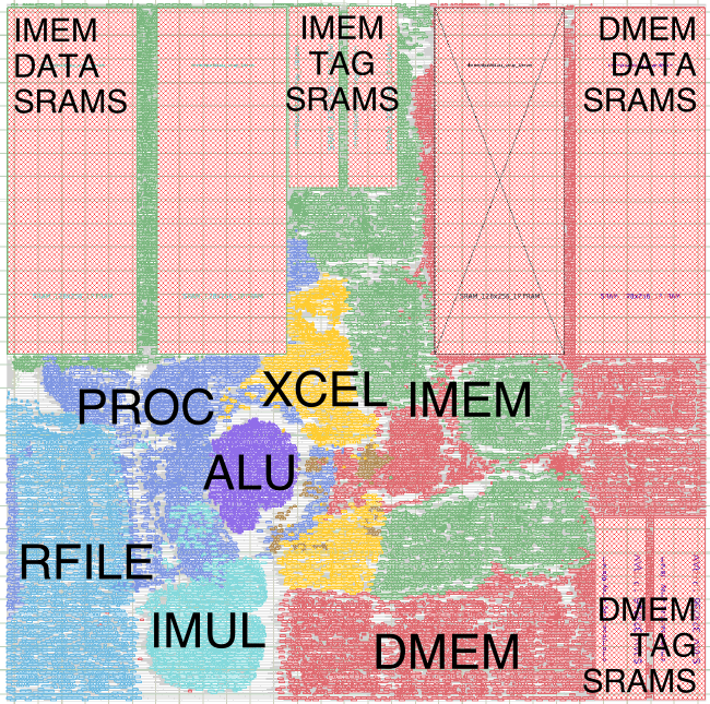
Here is the final summary of the performance, area, energy, and timing comparison between the pure-software vvadd microbenchmark and the accelerated vvadd microbenchmark. The accelerator seems to be a nice win in terms of energy, but we would probably need to invest further effort to improve the overall performance benefit.
| metric | pure-software | accelerated | relative |
|---|---|---|---|
| cycles | 1310 | 1111 | 1.18x |
| cycles* | 1012 | 817 | 1.23x |
| cycle time | 2.13 ns | 2.13 ns | 1.00x |
| area | 964,955 um^2 | 988,840 um^2 | 1.02x |
| energy | 156nJ | 72 nJ | 0.46x |
(*) assuming no cache misses
Using Verilog Accelerator RTL Models
Up until this point, we have been exclusively using PyMTL models for the processor, cache, and accelerator. PyMTL enables composition of pure-PyMTL and Verilog components, so it is also possible to compose a pure-PyMTL implementation of the processor and cache with a Verilog accelerator.
You can see a Verilog version of the vvadd accelerator in
sim/tut9_xcel/VvaddXcelVRTL.v. To switch to using this version, simply
change the rtl_language variable in sim/tut9_xcel/VvaddXcelRTL.py to
look like this:
rtl_language = 'pymtl'
Then we rerun the unit tests for the vvadd accelerator:
 % cd $TOPDIR/sim/build
 % pytest ../tut9_xcel
Then we can rerun the test and evaluation programs on the simulator with the Verilog version of the vvadd accelerator.
 % cd $TOPDIR/sim/build
 % ../pmx/pmx-sim --proc-impl rtl --cache-impl rtl --xcel-impl vvadd-rtl \
     ../../app/build/ubmark-vvadd-xcel-test1
 % ../pmx/pmx-sim --proc-impl rtl --cache-impl rtl --xcel-impl vvadd-rtl \
     --stats ../../app/build/ubmark-vvadd-xcel-eval
 num_cycles =  1111
The number of cycles is identical to what we saw with the PyMTL version of the vvadd accelerator, since both accelerators basically use the exact same design. Feel free to examine the line trace, which should be similar in spirit to what we saw with the PyMTL vvadd accelerator.
Finally, we can push the pure-PyMTL implementation of the processor and cache along with the Verilog implementation of the vvadd accelerator through the ASIC toolflow.
 % cd $TOPDIR/sim/build
 % ../pmx/pmx-sim --proc-impl rtl --cache-impl null --xcel-impl vvadd-rtl \
     --translate --dump-vtb ../../app/build/ubmark-vvadd-xcel-test1
 % ../pmx/pmx-sim --proc-impl rtl --cache-impl null --xcel-impl vvadd-rtl \
     --stats --translate --dump-vtb ../../app/build/ubmark-vvadd-xcel-eval

 % mkdir -p $TOPDIR/asic/build-tut9-pmx-vvadd
 % cd $TOPDIR/asic/build-tut9-pmx-vvadd
 % mflowgen run --design ../tut9-pmx-vvadd
 % make
The results should be similar to what we saw for the PyMTL version of the vvadd accelerator. You are free to implement your accelerators in this course using either PyMTL or Verilog.